Introduction to Multilayer PCB
A Printed Circuit Board (PCB) is the backbone of modern electronic devices. It provides a platform for mounting and interconnecting electronic components to create a functional circuit. As technology advances and devices become more complex, the need for higher density and more efficient PCBs has led to the development of multilayer PCBs.
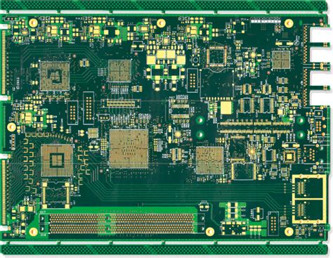
Multilayer PCBs are circuit boards that consist of three or more conductive layers laminated together with insulating material between each layer. These layers are interconnected through vias, which are small holes drilled through the board and plated with conductive material.
Advantages of Multilayer PCBs
Multilayer PCBs offer several advantages over single or double-layer boards:
-
Increased Density: Multilayer PCBs allow for a higher component density, as components can be placed on both sides of the board and interconnected through multiple layers.
-
Improved Signal Integrity: The use of ground and power planes in multilayer PCBs helps to reduce electromagnetic interference (EMI) and improve signal integrity.
-
Reduced Size: With the ability to accommodate more components in a smaller space, multilayer PCBs enable the design of compact and portable electronic devices.
-
Enhanced Reliability: The increased number of layers and the use of proper design techniques contribute to the overall reliability of the circuit.
Understanding the Layers in a Multilayer PCB
A typical multilayer PCB consists of several layers, each serving a specific purpose. Let’s explore these layers in detail.
Signal Layers
Signal layers are the layers on which the actual circuit traces are routed. These traces carry signals between components on the board. The number of signal layers in a multilayer PCB depends on the complexity of the circuit and the required signal density.
Power and Ground Planes
Power and ground planes are solid copper layers that provide a low-impedance path for power distribution and grounding. These planes help to minimize voltage drops, reduce EMI, and improve signal integrity. They also serve as reference planes for the signal layers.
Insulating Layers
Insulating layers, also known as dielectric layers, separate the conductive layers in a multilayer PCB. These layers are typically made of materials such as FR-4, which is a glass-reinforced epoxy laminate. The thickness and material properties of the insulating layers affect the electrical characteristics of the board, such as impedance and signal propagation.

Designing Multilayer PCBs
Designing a multilayer PCB requires careful consideration of various factors to ensure optimal performance and manufacturability. Here are some key aspects to consider when designing multilayer PCBs.
Layer Stackup
The layer stackup refers to the arrangement of conductive and insulating layers in a multilayer PCB. A well-designed layer stackup takes into account signal integrity, power distribution, and manufacturing constraints. It is essential to work closely with the PCB manufacturer to determine the appropriate layer stackup for your design.
Via Types and Placement
Vias are used to interconnect different layers in a multilayer PCB. There are several types of vias, including through-hole vias, blind vias, and buried vias. The choice of via type depends on the design requirements and manufacturing capabilities. Proper via placement is crucial to ensure signal integrity and avoid manufacturing issues.
Signal Integrity Considerations
Signal integrity is a critical aspect of multilayer PCB design. It involves ensuring that signals propagate through the board with minimal distortion, crosstalk, and noise. Some key considerations for signal integrity include:
- Trace width and spacing
- Impedance control
- Termination and matching
- Crosstalk reduction techniques
Thermal Management
As electronic devices become more powerful and compact, thermal management becomes increasingly important. Multilayer PCBs can generate significant heat, which needs to be dissipated effectively to ensure reliable operation. Thermal management techniques include the use of thermal vias, copper pours, and heat spreaders.

Manufacturing Multilayer PCBs
Manufacturing multilayer PCBs involves several steps, each requiring precise control and attention to detail. Here’s an overview of the manufacturing process:
-
Layer Fabrication: Each conductive layer is fabricated separately using a photolithographic process. The desired circuit pattern is transferred onto a copper-clad laminate using a photomask and then etched away.
-
Lamination: The fabricated layers are stacked together with insulating layers in between, and the entire stack is laminated under high temperature and pressure to form a solid board.
-
Drilling: Holes are drilled through the board to create vias and component mounting holes.
-
Plating: The drilled holes are plated with copper to create electrical connections between layers.
-
Solder Mask and Silkscreen: A solder mask is applied to the board to protect the copper traces from oxidation and prevent solder bridges during assembly. A silkscreen layer is added for component labeling and identification.
-
Surface Finish: A surface finish, such as HASL (Hot Air Solder Leveling) or ENIG (Electroless Nickel Immersion Gold), is applied to the exposed copper areas to improve solderability and protect against corrosion.

Testing and Inspection
To ensure the quality and reliability of multilayer PCBs, various testing and inspection techniques are employed. Some common methods include:
-
Automated Optical Inspection (AOI): AOI uses high-resolution cameras to inspect the board for manufacturing defects, such as missing components or solder bridges.
-
X-Ray Inspection: X-ray imaging is used to inspect the internal layers of the PCB for defects, such as voids or misaligned vias.
-
Electrical Testing: Electrical tests, such as continuity and insulation resistance tests, are performed to verify the electrical integrity of the board.
-
Functional Testing: The assembled board is tested under actual operating conditions to ensure proper functionality and performance.
Applications of Multilayer PCBs
Multilayer PCBs find applications in a wide range of industries and products. Some common applications include:
-
Consumer Electronics: Smartphones, tablets, laptops, and wearable devices heavily rely on multilayer PCBs to achieve compact and feature-rich designs.
-
Automotive Electronics: Modern vehicles incorporate numerous electronic systems, such as infotainment, navigation, and advanced driver assistance systems (ADAS), which require high-density multilayer PCBs.
-
Medical Devices: Medical equipment, such as diagnostic imaging systems and patient monitoring devices, utilize multilayer PCBs for reliable and precise operation.
-
Aerospace and Defense: Multilayer PCBs are used in avionics, satellite communication systems, and military equipment, where high reliability and performance are critical.
-
Industrial Automation: Industrial control systems, sensors, and automation equipment employ multilayer PCBs for robust and efficient operation in demanding environments.
Future Trends in Multilayer PCB Technology
As technology continues to advance, multilayer PCB technology is evolving to meet the growing demands of modern electronic devices. Some notable trends include:
-
High-Density Interconnect (HDI): HDI PCBs feature finer trace widths, smaller vias, and higher layer counts to achieve even greater component density and functionality.
-
Embedded Components: Embedding passive components, such as resistors and capacitors, within the PCB Layers helps to reduce board size and improve signal integrity.
-
Flexible and Rigid-flex PCBs: The use of flexible and rigid-flex PCBs allows for more creative and space-saving designs, particularly in wearable and portable devices.
-
Advanced Materials: New materials, such as low-loss dielectrics and high-temperature laminates, are being developed to meet the demands of high-speed and harsh-environment applications.
Frequently Asked Questions (FAQ)
-
Q: What is the difference between a multilayer PCB and a single-layer PCB?
A: A single-layer PCB has only one conductive layer, while a multilayer PCB consists of three or more conductive layers laminated together with insulating layers in between. Multilayer PCBs offer higher component density, improved signal integrity, and reduced board size compared to single-layer PCBs. -
Q: How many layers can a multilayer PCB have?
A: The number of layers in a multilayer PCB can vary depending on the complexity of the circuit and the manufacturing capabilities. Common layer counts range from 4 to 12 layers, but some advanced designs can have 20 or more layers. -
Q: What materials are used for the insulating layers in a multilayer PCB?
A: The most common material used for insulating layers in multilayer PCBs is FR-4, which is a glass-reinforced epoxy laminate. Other materials, such as polyimide or high-frequency laminates, may be used for specific applications or performance requirements. -
Q: What are the advantages of using blind and buried vias in a multilayer PCB?
A: Blind and buried vias help to conserve board space and improve signal integrity by providing more direct connections between layers. Blind vias connect an outer layer to an inner layer, while buried vias connect two or more inner layers without reaching the outer layers. -
Q: How can I ensure the manufacturability of my multilayer PCB design?
A: To ensure manufacturability, it is essential to follow the design guidelines provided by your PCB manufacturer. This includes adhering to minimum trace widths, spacings, and via sizes, as well as considering the capabilities and limitations of the manufacturing process. Early collaboration with the manufacturer can help to identify and address any potential issues before production.
Conclusion
Multilayer PCBs have revolutionized the electronics industry by enabling the design of compact, high-performance, and reliable electronic devices. By understanding the layers, design considerations, manufacturing process, and testing techniques involved in multilayer PCBs, engineers can create innovative and robust electronic products.
As technology advances, multilayer PCB technology will continue to evolve, pushing the boundaries of what is possible in electronic design. By staying up-to-date with the latest trends and best practices, designers can leverage the full potential of multilayer PCBs to create cutting-edge electronic solutions.
No responses yet