Introduction to PCB Manufacturing
Printed circuit boards (PCBs) are essential components in virtually all modern electronic devices, from smartphones and laptops to medical equipment and aerospace systems. The process of creating these complex boards involves two main stages: PCB fabrication and PCB Assembly. Although these terms are often used interchangeably, they refer to distinct phases in the PCB manufacturing process, each with its own set of procedures, equipment, and challenges. Understanding the difference between PCB fabrication and assembly is crucial for anyone involved in electronics design, manufacturing, or procurement.
What is PCB Fabrication?
PCB fabrication, also known as PCB manufacturing or printing, is the process of creating the bare printed circuit board. This involves transforming a raw substrate material, typically a copper-clad laminate (CCL), into a fully functional PCB with conductive traces, pads, and other features. The fabrication process can be broken down into several key steps:
1. PCB Design and Gerber File Generation
Before fabrication can begin, the PCB must be designed using specialized electronic design automation (EDA) software. The design includes the board’s schematic, component layout, and routing of conductive traces. Once the design is finalized, Gerber files are generated, which contain all the necessary information for manufacturing the PCB, such as the copper layer patterns, drill holes, and solder mask openings.
2. Substrate Preparation
The substrate, typically a fiberglass-reinforced epoxy resin (FR-4), is cut to the desired size and shape. If the design requires multiple layers, additional substrates are prepared, and the copper foil is laminated onto both sides of each substrate.
3. Copper Patterning
The copper layer is selectively removed to create the desired conductive pattern. This is typically done using a photolithographic process:
a. The copper surface is cleaned and coated with a light-sensitive photoresist.
b. The Gerber file’s copper layer pattern is transferred onto a photomask or film.
c. The photoresist is exposed to UV light through the photomask, hardening the exposed areas.
d. The unexposed photoresist is removed using a developer solution, leaving the desired copper pattern protected.
e. The exposed copper is etched away using a chemical solution, typically cupric chloride or ammonium persulfate.
f. The remaining photoresist is stripped off, revealing the final copper pattern.
4. Lamination and Drilling
For multi-layer PCBs, the patterned layers are aligned and laminated together under high pressure and temperature. The resulting board is then drilled to create through-holes and vias that connect the different layers.
5. Surface Finishes and Solder Mask Application
To protect the copper traces from oxidation and facilitate soldering, a surface finish is applied to the PCB. Common surface finishes include:
| Finish | Composition | Advantages | Disadvantages |
|---|---|---|---|
| HASL | Hot Air Solder Leveling (Tin/Lead) | Low cost, good solderability | Uneven surface, contains lead |
| ENIG | Electroless Nickel Immersion Gold | Flat surface, good solderability, RoHS-Compliant | Higher cost, possible “black pad” issue |
| OSP | Organic Solderability Preservative | Low cost, flat surface, RoHS-compliant | Limited shelf life, weak copper adhesion |
| Immersion Silver | Immersion Silver | Low cost, good solderability, RoHS-compliant | Tarnishes over time, weak copper adhesion |
A solder mask, usually a green epoxy-based ink, is then applied to the PCB, covering the areas that should not be soldered. This helps to prevent short circuits and improves the board’s appearance.
6. Silkscreen and Final Inspection
Finally, a silkscreen layer is added to the PCB, which includes text, logos, and component identifiers to aid in assembly and debugging. The fabricated PCB undergoes a thorough inspection to ensure it meets the required specifications before being packaged and shipped for assembly.

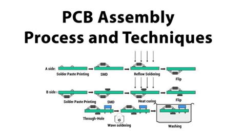
What is PCB Assembly?
PCB assembly, also known as PCB population or PCB stuffing, is the process of attaching electronic components to the fabricated PCB. This stage transforms the bare board into a functional electronic assembly ready for integration into the final product. PCB assembly involves several key steps:
1. Component Procurement and Preparation
The first step in PCB assembly is to procure the necessary components, such as integrated circuits (ICs), resistors, capacitors, and connectors. The components are then prepared for assembly by programming (if required), forming leads, and applying any necessary coatings or treatments.
2. Solder Paste Application
For surface mount devices (SMDs), solder paste is applied to the PCB’s pads using a stencil or screen printing process. The solder paste consists of tiny solder spheres suspended in a flux medium, which helps to clean the metal surfaces and prevent oxidation during soldering.
3. Component Placement
The prepared components are placed onto the PCB using automated pick-and-place machines or manual assembly methods. Precise placement is crucial to ensure proper electrical connections and avoid component damage during soldering.
4. Soldering
The populated PCB is then sent through a reflow oven, which heats the board to a specific temperature profile, melting the solder paste and forming permanent electrical and mechanical connections between the components and the PCB. For through-hole components, wave soldering or selective soldering techniques may be used instead.
5. Inspection and Testing
After soldering, the assembled PCB undergoes visual inspection and automated optical inspection (AOI) to identify any defects, such as missing or misaligned components, solder bridges, or insufficient solder joints. Functional testing is also performed to ensure the board operates as intended.
6. Rework and Repair
If any issues are found during inspection or testing, the PCB may require rework or repair. This involves removing and replacing faulty components, correcting solder joint issues, and resolving any other problems that may affect the board’s functionality.
7. Conformal Coating and Final Assembly
Depending on the application, the assembled PCB may be coated with a protective conformal coating to shield it from moisture, dust, and other environmental factors. The board is then integrated into the final product or packaged for shipment.

PCB Fabrication vs Assembly: Key Differences
While PCB fabrication and assembly are both essential stages in the PCB manufacturing process, they involve distinct procedures, equipment, and challenges. Some key differences between PCB fabrication and assembly include:
-
Focus: PCB fabrication focuses on creating the bare board with conductive traces and features, while PCB assembly focuses on populating the board with components and ensuring proper functionality.
-
Equipment: PCB fabrication relies on specialized equipment for substrate preparation, copper patterning, drilling, and surface finishing, while PCB assembly uses pick-and-place machines, reflow ovens, and soldering tools.
-
Materials: PCB fabrication primarily deals with substrates, copper foil, and chemical solutions, while PCB assembly involves a wide range of electronic components, solder paste, and coatings.
-
Skill Sets: PCB fabrication requires expertise in chemical processes, photolithography, and material science, while PCB assembly demands knowledge of component specifications, soldering techniques, and quality control.
-
Lead Time: PCB fabrication typically has a longer lead time than assembly, as it involves more complex and time-consuming processes, such as multi-layer lamination and drill hole plating.

FAQ
1. Can PCB fabrication and assembly be done by the same company?
Yes, many PCB manufacturers offer both fabrication and assembly services, providing a one-stop solution for customers. This can streamline the production process and reduce lead times, as the fabricated boards can be directly transferred to the assembly line without the need for shipping to another facility.
2. What are the advantages of outsourcing PCB fabrication and assembly?
Outsourcing PCB fabrication and assembly to specialized manufacturers offers several advantages, including:
– Access to state-of-the-art equipment and expertise
– Lower production costs due to economies of scale
– Faster turnaround times and higher production capacity
– Improved quality control and reliability
– Flexibility to focus on core competencies and product development
3. How do I choose a reliable PCB fabrication and assembly partner?
When selecting a PCB fabrication and assembly partner, consider the following factors:
– Experience and expertise in your specific industry or application
– Quality certifications, such as ISO 9001, AS9100, or IPC standards
– Production capabilities, including board complexity, layer count, and material options
– Lead times, pricing, and minimum order quantities
– Customer support, communication, and responsiveness
– References and customer testimonials
4. What are the common challenges in PCB fabrication and assembly?
Some common challenges in PCB fabrication and assembly include:
– Ensuring accurate and consistent copper patterning and etching
– Achieving reliable multi-layer lamination and registration
– Handling and placing miniature or delicate components
– Maintaining proper solder joint quality and preventing defects
– Managing lead times and inventory for components with long lead times or limited availability
– Complying with regulatory requirements, such as RoHS and REACH
5. How can I optimize my PCB design for fabrication and assembly?
To optimize your PCB design for fabrication and assembly, consider the following best practices:
– Adhere to the manufacturer’s design guidelines and constraints
– Use standard component sizes and packaging where possible
– Provide clear and accurate documentation, including Gerber files, bill of materials (BOM), and assembly drawings
– Allow for adequate spacing between components and traces to facilitate soldering and inspection
– Select appropriate surface finishes and solder mask options based on the application and assembly process
– Conduct design for manufacturability (DFM) and design for assembly (DFA) reviews to identify and address potential issues early in the design process
Conclusion
PCB fabrication and assembly are two critical stages in the PCB manufacturing process, each with its own set of procedures, equipment, and challenges. Understanding the differences between these stages is essential for anyone involved in electronics design, manufacturing, or procurement. By working with experienced and reliable PCB fabrication and assembly partners, optimizing designs for manufacturability and assembly, and staying informed about the latest technologies and best practices, companies can ensure the successful production of high-quality, reliable PCBs for their electronic products.
No responses yet