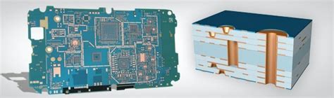
What are HDI PCBs?
HDI PCBs are a type of printed circuit board that features higher wiring density per unit area compared to conventional PCBs. This is achieved through the use of smaller vias, finer trace widths and spaces, and advanced manufacturing techniques. HDI PCBs allow for the miniaturization of electronic devices while maintaining or enhancing their functionality and performance.
The main characteristics of HDI PCBs include:
– Smaller vias (microvias) with diameters less than 150 microns
– Finer trace widths and spaces, typically less than 100 microns
– Higher layer counts (8 or more layers)
– Buried and blind vias for increased routing density
– Sequential lamination process for fabrication
Benefits of HDI PCBs
Miniaturization
One of the primary advantages of HDI PCBs is their ability to enable the miniaturization of electronic devices. With the use of smaller components and denser wiring, HDI PCBs can significantly reduce the size and weight of electronic products. This is particularly important for portable devices such as smartphones, smartwatches, and medical wearables, where compact design is a key selling point.
Enhanced Performance
HDI PCBs offer improved electrical performance compared to traditional PCBs. The shorter signal paths and reduced parasitic capacitance and inductance result in faster signal transmission, lower signal loss, and reduced electromagnetic interference (EMI). This makes HDI PCBs ideal for high-speed applications, such as 5G networks, high-frequency radar systems, and high-performance computing.
Increased Functionality
The higher wiring density of HDI PCBs allows for the integration of more components and features into a single board. This enables the development of multifunctional devices that can perform various tasks, such as a smartphone that serves as a camera, music player, and GPS navigation system. HDI PCBs also facilitate the implementation of advanced packaging techniques, such as System-in-Package (SiP) and Package-on-Package (PoP), which further enhance the functionality and performance of electronic devices.
Cost-Effectiveness
Although HDI PCBs have higher initial design and manufacturing costs compared to conventional PCBs, they can be more cost-effective in the long run. The miniaturization and increased functionality enabled by HDI PCBs can lead to reduced overall system costs, as fewer components and less packaging are required. Additionally, the improved reliability and performance of HDI PCBs can result in lower maintenance and replacement costs over the product’s lifetime.

HDI PCB Manufacturing Process
The manufacturing process for HDI PCBs is more complex and precise than that of traditional PCBs. It involves advanced techniques and specialized equipment to achieve the high wiring density and small feature sizes required. The main steps in the HDI PCB manufacturing process are:
-
Design and Layout: The HDI PCB design is created using computer-aided design (CAD) software, taking into account the specific requirements of the intended application. The layout is optimized for high-density wiring and component placement, utilizing microvias, fine traces, and buried/blind vias as necessary.
-
Material Selection: The base material for HDI PCBs is typically a high-performance laminate, such as polyimide or liquid crystal polymer (LCP), which offers excellent electrical and thermal properties. The copper foil used for the conductive layers is also thinner than that used in conventional PCBs, typically 1/2 oz or less.
-
Drilling and Plating: The microvias are drilled using laser or mechanical drilling techniques, depending on the via size and depth required. The vias are then plated with copper to create electrical connections between layers. For HDI PCBs with buried or blind vias, a sequential lamination process is used to build up the layers one at a time.
-
Patterning and Etching: The conductive layers are patterned using photolithography, where a photoresist is applied, exposed, and developed to create the desired trace pattern. The unwanted copper is then etched away using a chemical etching process, leaving the fine traces and pads intact.
-
Lamination: The patterned layers are laminated together using heat and pressure to form a solid board. For HDI PCBs with multiple lamination cycles, the process is repeated for each additional layer.
-
Surface Finishing: The exposed copper surfaces are coated with a protective finish, such as immersion gold (ENIG) or organic solderability preservative (OSP), to prevent oxidation and improve solderability.
-
Solder Mask and Silkscreen: A solder mask is applied to the board to protect the traces and prevent solder bridging during assembly. A silkscreen layer is then added to provide component labels and other markings.
-
Electrical Testing: The completed HDI PCB undergoes thorough electrical testing to ensure that all connections are properly formed and that there are no short circuits or open connections. This may include automated optical inspection (AOI), in-circuit testing (ICT), and functional testing.

Applications of HDI PCBs
HDI PCBs find applications in a wide range of industries and products where miniaturization, high performance, and advanced functionality are required. Some of the key application areas include:
Consumer Electronics
- Smartphones and tablets
- Smartwatches and fitness trackers
- Digital cameras and video recorders
- Gaming consoles and controllers
Medical Devices
- Implantable devices (pacemakers, neurostimulators)
- Wearable health monitors
- Portable medical instruments
- Diagnostic imaging equipment
Automotive Electronics
- Advanced driver assistance systems (ADAS)
- In-vehicle infotainment systems
- Electronic control units (ECUs)
- Sensor and actuator modules
Aerospace and Defense
- Avionics systems
- Satellite communication devices
- Radar and surveillance equipment
- Military wearables and portable devices
Industrial Automation
- Robotics and motion control systems
- Industrial IoT devices and sensors
- Process control and monitoring equipment
- Wireless communication modules

Challenges and Future Trends
While HDI PCBs offer numerous benefits, they also present some challenges in design, manufacturing, and assembly. Some of the key challenges include:
-
Design Complexity: HDI PCBs require careful design and layout to ensure optimal signal integrity, thermal management, and manufacturability. Designers must have a deep understanding of HDI design rules and constraints, as well as the ability to use advanced CAD tools and simulation software.
-
Manufacturing Precision: The small feature sizes and high wiring density of HDI PCBs demand strict process control and precision in manufacturing. This requires specialized equipment, such as laser drills and high-resolution photolithography systems, as well as skilled operators and technicians.
-
Assembly Challenges: The small component sizes and fine pitch of HDI PCBs can make assembly more difficult and time-consuming. Advanced assembly techniques, such as surface mount technology (SMT) and chip-on-board (COB), are often required, along with specialized equipment and processes for handling and inspection.
Despite these challenges, the demand for HDI PCBs is expected to continue growing in the coming years, driven by the increasing complexity and miniaturization of electronic devices. Some of the future trends in HDI PCB technology include:
-
Advanced Materials: The development of new laminate materials with improved electrical, thermal, and mechanical properties will enable the production of HDI PCBs with even higher performance and reliability.
-
Embedded Components: The integration of passive components (resistors, capacitors) and active components (ICs) directly into the PCB substrate will further increase the density and functionality of HDI PCBs.
-
3D Printing: The use of additive manufacturing techniques, such as 3D printing, for the fabrication of HDI PCBs could enable faster prototyping, greater design flexibility, and the creation of complex, three-dimensional structures.
-
Advanced Packaging: The adoption of advanced packaging techniques, such as fan-out wafer-level packaging (FOWLP) and 2.5D/3D IC packaging, will drive the development of HDI PCBs with even higher interconnect densities and performance.
FAQ
1. What is the difference between HDI PCBs and conventional PCBs?
HDI PCBs have higher wiring density per unit area compared to conventional PCBs. They feature smaller vias (microvias), finer trace widths and spaces, higher layer counts, and advanced manufacturing techniques such as sequential lamination. This enables the miniaturization and enhanced performance of electronic devices.
2. What are the main benefits of using HDI PCBs?
The main benefits of using HDI PCBs include:
– Miniaturization of electronic devices
– Enhanced electrical performance (faster signal transmission, lower signal loss, reduced EMI)
– Increased functionality through integration of more components and features
– Cost-effectiveness in the long run due to reduced system costs and improved reliability
3. What industries and applications commonly use HDI PCBs?
HDI PCBs are commonly used in various industries and applications where miniaturization, high performance, and advanced functionality are required. These include consumer electronics (smartphones, tablets), medical devices (implantables, wearables), automotive electronics (ADAS, infotainment systems), aerospace and defense (avionics, radar systems), and industrial automation (robotics, IoT devices).
4. What are the main challenges in designing and manufacturing HDI PCBs?
The main challenges in designing and manufacturing HDI PCBs include:
– Design complexity, requiring a deep understanding of HDI design rules and constraints
– Manufacturing precision, demanding strict process control and specialized equipment
– Assembly challenges, such as handling small components and fine pitch, requiring advanced techniques and processes
5. What are some of the future trends in HDI PCB technology?
Some of the future trends in HDI PCB technology include the development of advanced materials with improved properties, the integration of embedded components, the use of 3D printing for faster prototyping and greater design flexibility, and the adoption of advanced packaging techniques such as fan-out wafer-level packaging and 2.5D/3D IC packaging.
| Feature | Conventional PCBs | HDI PCBs |
|---|---|---|
| Via Diameter | > 150 microns | < 150 microns |
| Trace Width and Spacing | > 100 microns | < 100 microns |
| Layer Count | Typically < 8 | Typically ≥ 8 |
| Via Types | Through-hole | Buried, blind |
| Manufacturing Process | Standard | Sequential lamination |
In conclusion, High-Density Interconnect (HDI) Printed Circuit Boards have become an essential component in the development of advanced electronic devices. Their ability to enable miniaturization, enhance performance, increase functionality, and provide cost-effectiveness has made them indispensable in various industries, from consumer electronics to medical devices and aerospace systems. As technology continues to evolve and the demand for more compact and high-performance devices grows, HDI PCBs will play an increasingly crucial role in shaping the future of electronics.
No responses yet