What are PCBs?
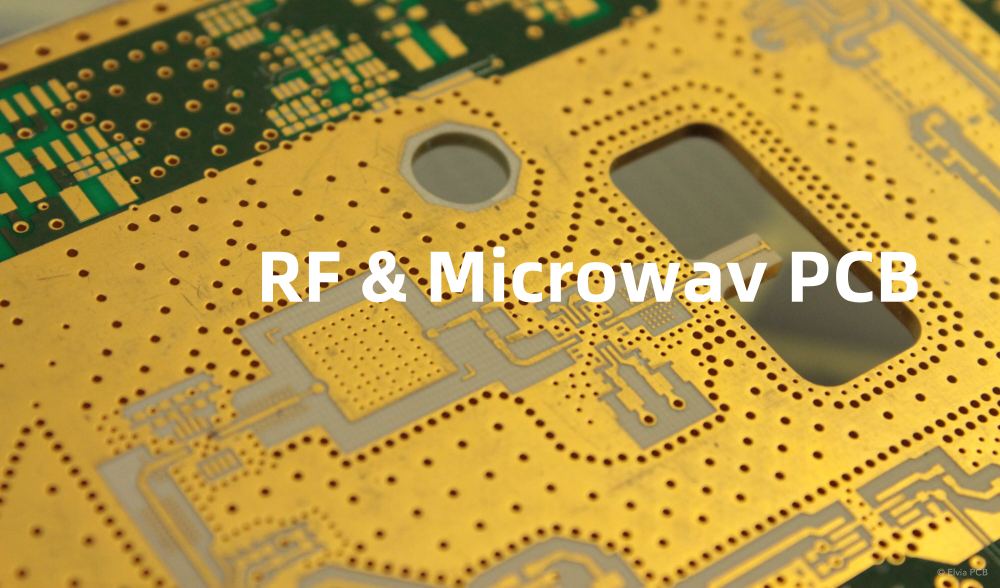
PCBs are flat boards made of insulating materials, such as fiberglass or plastic, with conductive copper traces printed on them. These traces connect various electronic components, such as resistors, capacitors, and integrated circuits (ICs), to form a complete electronic circuit. PCBs provide a stable and reliable platform for these components, allowing for compact and efficient designs.
History of PCBs
The concept of PCBs dates back to the early 20th century when inventors began exploring ways to simplify the wiring of electronic devices. However, it wasn’t until the 1940s that the first true PCBs were developed. During World War II, the U.S. military needed a reliable and compact way to connect electronic components in their radar systems. This led to the invention of the “printed wire board,” which laid the foundation for modern PCBs.
In the 1950s, the PCB manufacturing process was refined, and the use of PCBs began to spread to consumer electronics. The introduction of through-hole technology, which involved drilling holes in the PCB and inserting component leads through them, made it easier to assemble and solder components onto the board.
The 1960s and 1970s saw the rise of surface-mount technology (SMT), which allowed for even smaller and more densely packed PCBs. With SMT, components were soldered directly onto the surface of the PCB, eliminating the need for through-holes.
Today, PCBs are an integral part of the electronics industry, with advanced manufacturing techniques and materials enabling the creation of highly complex and reliable boards.
PCB Manufacturing Process
The PCB manufacturing process involves several steps, each critical to ensuring the quality and reliability of the final product. Here’s a brief overview of the main stages:
-
Design: The PCB design is created using specialized software, such as Eagle or KiCad. The designer determines the placement of components, routing of traces, and other essential features.
-
Printing: The PCB design is printed onto a transparent film or directly onto the copper-clad board using a photoplotter or laser printer.
-
Etching: The printed board is exposed to UV light, which hardens the areas not covered by the printed design. The board is then placed in an etching solution, which removes the unwanted copper, leaving only the desired traces.
-
Drilling: Holes are drilled into the board to accommodate through-hole components or to create vias, which connect traces on different layers of the PCB.
-
Plating: A thin layer of copper is deposited onto the board and into the drilled holes to ensure proper electrical conductivity.
-
Solder mask application: A protective layer, known as the solder mask, is applied to the board to prevent accidental short circuits and to protect the copper traces from oxidation.
-
Silkscreen printing: Text, logos, and other markings are printed onto the board using a silkscreen process to aid in assembly and identification of components.
-
Surface finish: A surface finish, such as HASL (Hot Air Solder Leveling) or ENIG (Electroless Nickel Immersion Gold), is applied to the exposed copper to prevent oxidation and improve solderability.
-
Assembly: Components are placed and soldered onto the PCB, either manually or using automated pick-and-place machines.
-
Testing: The assembled PCB undergoes various tests, such as continuity, functionality, and burn-in tests, to ensure proper operation and reliability.
PCB Design Considerations
When designing a PCB, several factors must be taken into account to ensure optimal performance and reliability. Some of the key considerations include:
Component placement
The placement of components on the PCB is crucial for several reasons:
- Signal integrity: Proper component placement minimizes the distance between connected components, reducing signal loss and interference.
- Thermal management: Components that generate significant heat should be placed in a way that allows for adequate cooling, such as near the edge of the board or with sufficient spacing between them.
- Mechanical stability: Heavy or tall components should be placed in a manner that minimizes stress on the board and prevents damage during handling or operation.
Trace routing
The routing of traces on the PCB is another critical aspect of design. Some important factors to consider include:
- Trace width: The width of the traces should be appropriate for the current they will carry. Wider traces are needed for higher currents to prevent excessive heating and voltage drop.
- Trace spacing: Adequate spacing between traces is necessary to prevent crosstalk and signal interference. The spacing depends on factors such as the signal frequency and the dielectric constant of the PCB material.
- Trace length: Minimizing trace length is essential for reducing signal loss and improving signal integrity. This is particularly important for high-frequency signals.
Grounding and shielding
Proper grounding and shielding techniques are essential for minimizing electromagnetic interference (EMI) and ensuring the stability of the circuit. Some key considerations include:
- Ground planes: Using solid ground planes on one or more layers of the PCB can provide a low-impedance return path for signals and help reduce EMI.
- Shielding: Sensitive components or regions of the PCB can be shielded using conductive enclosures or by placing them on inner layers of the board, surrounded by ground planes.
- Decoupling capacitors: Placing decoupling capacitors close to ICs and other active components can help reduce high-frequency noise and ensure a stable power supply.
Layer stack-up
The number and arrangement of layers in a PCB can have a significant impact on its performance and cost. Some factors to consider when deciding on the layer stack-up include:
- Signal layers: The number of signal layers required depends on the complexity of the circuit and the number of components. More layers allow for greater routing flexibility but also increase the cost of the PCB.
- Power and ground planes: Dedicated power and ground planes can provide a stable and low-impedance supply to the components, improving signal integrity and reducing EMI.
- Dielectric thickness: The thickness of the dielectric material between layers affects the impedance of the traces and the overall thickness of the PCB. Thinner dielectrics allow for smaller vias and tighter trace spacing but can also increase the cost of the board.

PCB Applications
PCBs are used in a wide range of applications across various industries. Some common examples include:
Consumer electronics
PCBs are found in nearly all consumer electronic devices, such as:
- Smartphones and tablets
- Laptops and desktop computers
- Televisions and displays
- Gaming consoles and controllers
- Wearable devices
Industrial electronics
PCBs play a crucial role in industrial applications, including:
- Process control systems
- Automation and robotics
- Power electronics and motor drives
- Instrumentation and measurement equipment
Medical devices
PCBs are essential components in various medical devices, such as:
- Diagnostic equipment (e.g., MRI, CT scanners)
- Monitoring systems (e.g., ECG, EEG)
- Implantable devices (e.g., pacemakers, neurostimulators)
- Surgical instruments
Automotive electronics
Modern vehicles rely heavily on PCBs for various systems, including:
- Engine control units (ECUs)
- Infotainment systems
- Advanced driver assistance systems (ADAS)
- Lighting and climate control
Aerospace and defense
PCBs used in aerospace and defense applications must meet stringent reliability and environmental requirements. Examples include:
- Avionics systems
- Satellite communication equipment
- Radar and surveillance systems
- Missile guidance and control
Future Trends in PCB Technology
As electronics continue to evolve, so do PCBs. Some of the emerging trends in PCB technology include:
Miniaturization
The demand for smaller, more compact electronic devices is driving the development of advanced PCB manufacturing techniques, such as:
- High-density interconnect (HDI) PCBs
- Embedded components
- 3D printing of PCBs
Flexible and stretchable PCBs
Flexible and stretchable PCBs are gaining popularity in applications that require conformity to non-planar surfaces or the ability to withstand repeated bending and stretching, such as:
- Wearable electronics
- Medical implants
- Soft robotics
High-speed and high-frequency PCBs
As data rates and signal frequencies continue to increase, PCBs must be designed to minimize signal loss and distortion. Some techniques used in high-speed and high-frequency PCB design include:
- Controlled impedance traces
- Low-loss dielectric materials
- Advanced via structures (e.g., blind and buried vias)
Environmentally friendly materials
There is a growing emphasis on using environmentally friendly materials in PCB manufacturing to reduce the industry’s ecological impact. Some examples include:
- Halogen-free flame retardants
- Lead-free solders
- Biodegradable and recyclable PCB substrates
Frequently Asked Questions (FAQ)
- What is the difference between a single-sided and a double-sided PCB?
-
A single-sided PCB has conductive traces on only one side of the board, while a double-sided PCB has traces on both sides. Double-sided PCBs offer more routing flexibility and higher component density but are also more expensive to manufacture.
-
What is the purpose of a solder mask on a PCB?
-
The solder mask is a protective layer applied to the PCB that covers the copper traces, leaving only the pads and other areas that need to be soldered exposed. It prevents accidental short circuits, protects the traces from oxidation, and provides electrical insulation.
-
What is the difference between through-hole and surface-mount components?
-
Through-hole components have leads that are inserted into holes drilled in the PCB and soldered on the opposite side. Surface-mount components are soldered directly onto pads on the surface of the PCB. Surface-mount components are generally smaller and allow for higher component density, while through-hole components are often used for larger or higher-power components.
-
What is a via in a PCB?
-
A via is a small hole drilled in the PCB that connects traces on different layers of the board. Vias can be through-hole (going through the entire board), blind (connecting an outer layer to an inner layer), or buried (connecting inner layers only).
-
How can I ensure my PCB design is manufacturable?
- To ensure your PCB design is manufacturable, consider the following:
- Adhere to the design rules and guidelines provided by your PCB manufacturer, such as minimum trace widths, clearances, and drill sizes.
- Use standard component sizes and footprints whenever possible.
- Avoid overly complex or dense designs that may be difficult or expensive to manufacture.
- Communicate with your PCB manufacturer early in the design process to identify any potential issues or limitations.
In conclusion, understanding the fundamentals of PCBs is essential for anyone involved in electronics design and manufacturing. From their history and manufacturing process to design considerations and applications, PCBs play a critical role in enabling the creation of compact, reliable, and high-performance electronic devices. As technology continues to advance, staying up-to-date with the latest trends and techniques in PCB design and manufacturing will be crucial for success in this ever-evolving field.

No responses yet