Introduction to PCB Manufacturing
Printed Circuit Board (PCB) manufacturing is a complex process that involves several steps to create a functional and reliable electronic circuit. PCBs are the backbone of modern electronics, found in everything from smartphones and computers to medical devices and aerospace systems. As technology advances, the demand for high-quality, cost-effective, and rapidly produced PCBs continues to grow.
In this article, we will explore the PCB manufacturing process in detail, discussing key aspects such as design, material selection, fabrication techniques, assembly methods, and quality control. We will also provide insights on how to optimize the PCB manufacturing process for better results and address frequently asked questions related to PCB production.
The PCB Manufacturing Process
Step 1: PCB Design and Layout
The first step in PCB manufacturing is designing the circuit and creating a layout. This involves using specialized software tools to create a schematic diagram of the electronic components and their interconnections. The schematic is then translated into a physical layout, which determines the placement of components and routing of copper traces on the PCB.
Key considerations during PCB design include:
- Component selection and placement
- Signal integrity and electromagnetic compatibility
- Power distribution and thermal management
- Manufacturing constraints and design for manufacturability (DFM)
Step 2: Material Selection
The choice of materials for PCB manufacturing depends on the specific requirements of the application, such as electrical properties, thermal stability, mechanical strength, and cost. The most common materials used in PCB production are:
| Material | Description | Applications |
|---|---|---|
| FR-4 | Glass-reinforced epoxy laminate | General-purpose, high-volume PCBs |
| Polyimide | High-temperature, flexible substrate | Aerospace, military, and medical devices |
| Aluminum | Metal-core substrate for heat dissipation | High-power LED lighting, automotive electronics |
| Rogers | High-frequency, low-loss dielectric materials | RF and microwave applications |
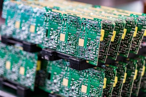
Step 3: PCB Fabrication
PCB fabrication involves several sub-processes to create the physical board from the design files. These sub-processes include:
-
Printing: The PCB layout is printed onto a photosensitive film or directly onto the copper-clad laminate using a high-resolution printer.
-
Exposure and Development: The printed film is used as a mask to expose the photoresist-coated copper layer to UV light. The exposed areas of the photoresist are then removed using a chemical developer, leaving behind a pattern of copper traces.
-
Etching: The exposed copper areas are removed using a chemical etching process, typically with an acidic solution like ferric chloride or ammonium persulfate.
-
Drilling: Holes are drilled through the PCB to accommodate through-hole components and create vias for interconnecting layers in multi-layer boards.
-
Plating: The drilled holes are plated with copper to create electrical connections between layers and provide a surface for soldering components.
-
Solder Mask Application: A protective solder mask is applied to the PCB surface, leaving only the exposed pads and contacts for soldering components.
-
Silkscreen Printing: A silkscreen layer is printed onto the PCB to add component labels, logos, and other markings for assembly and identification purposes.
Step 4: PCB Assembly
Once the bare PCB is fabricated, the next step is to assemble the electronic components onto the board. There are two primary methods for PCB assembly:
-
Through-Hole Assembly (THA): Components with long leads are inserted through holes in the PCB and soldered onto the opposite side. THA is suitable for larger components and provides strong mechanical connections.
-
Surface Mount Assembly (SMT): Components with small, flat contacts are placed directly onto pads on the PCB surface and soldered using a reflow oven. SMT allows for higher component density and faster assembly compared to THA.
The choice of assembly method depends on factors such as component availability, board size, production volume, and cost considerations.
Step 5: Quality Control and Testing
To ensure the reliability and functionality of the manufactured PCBs, several quality control and testing procedures are carried out at various stages of the production process. These include:
- Visual inspection for defects and workmanship
- Automated optical inspection (AOI) for component placement and solder joint quality
- X-ray inspection for hidden defects in multi-layer boards
- In-circuit testing (ICT) for verifying component functionality and connectivity
- Functional testing to validate the overall performance of the assembled PCB

Optimizing PCB Manufacturing for Better Results
To improve the efficiency, quality, and cost-effectiveness of PCB manufacturing, consider the following best practices:
-
Design for Manufacturing (DFM): Incorporate DFM principles early in the design process to ensure compatibility with manufacturing processes and minimize the risk of defects and delays.
-
Standardization: Use standardized components, materials, and processes wherever possible to reduce costs, improve availability, and streamline production.
-
Automated Processes: Invest in automated equipment and software tools for PCB design, fabrication, and assembly to increase productivity, reduce human errors, and improve consistency.
-
Continuous Improvement: Regularly review and optimize the PCB manufacturing process based on feedback from quality control, customer requirements, and industry best practices.
-
Collaboration and Communication: Foster close collaboration and clear communication among design, manufacturing, and quality teams to identify and resolve issues quickly and efficiently.

Frequently Asked Questions (FAQ)
-
What is the typical lead time for PCB manufacturing?
The lead time for PCB manufacturing varies depending on factors such as board complexity, material availability, and production volume. Typical lead times range from a few days for simple, prototype boards to several weeks for complex, high-volume production runs. -
How much does PCB manufacturing cost?
PCB manufacturing costs depend on various factors, including board size, layer count, material type, component density, and production volume. Small, simple boards can cost a few dollars each, while large, complex boards can cost hundreds of dollars per unit. Economies of scale and design optimization can help reduce overall costs. -
What are the most common PCB manufacturing defects?
Some of the most common PCB manufacturing defects include: - Shorts and opens in copper traces
- Incorrect component placement or orientation
- Poor solder joint quality, such as bridging, voids, or cold joints
- Delamination or warping of the board substrate
-
Inconsistent or incomplete plating in holes and vias
-
How can I ensure the quality and reliability of my PCBs?
To ensure the quality and reliability of your PCBs, follow these guidelines: - Implement a robust design for manufacturing (DFM) process
- Use high-quality materials and components from reputable suppliers
- Adhere to industry standards and best practices for PCB fabrication and assembly
- Conduct thorough quality control and testing at various stages of production
-
Work with experienced and certified PCB manufacturers with a proven track record
-
What are the environmental considerations in PCB manufacturing?
PCB manufacturing involves the use of chemicals and materials that can have environmental impacts if not properly managed. Key environmental considerations include: - Proper handling, storage, and disposal of chemicals used in fabrication processes
- Compliance with regulations on hazardous substances, such as RoHS and REACH
- Implementing eco-friendly practices, such as recycling, waste reduction, and energy efficiency
- Choosing materials and processes with lower environmental footprints, such as halogen-free laminates and lead-free solders

Conclusion
PCB manufacturing is a complex and critical process that directly impacts the performance, reliability, and cost of electronic products. By understanding the various stages of PCB production, from design and material selection to fabrication, assembly, and quality control, engineers and manufacturers can optimize the process for better results.
Implementing best practices such as design for manufacturability, standardization, automation, continuous improvement, and collaboration can help streamline PCB manufacturing, reduce defects, and improve overall quality. As technology continues to advance, staying up-to-date with the latest trends, techniques, and regulations in PCB manufacturing will be essential for success in the competitive electronics industry.
No responses yet