Introduction to PCB History
The printed circuit board (PCB) has revolutionized the electronics industry since its inception. It has become an essential component in virtually every electronic device we use today, from smartphones and computers to medical equipment and aerospace technology. The history of the PCB is a fascinating journey that spans over a century, marked by innovative discoveries, technological advancements, and the relentless pursuit of miniaturization and efficiency. In this article, we will delve into the rich history of the PCB, tracing its evolution from the early days of electrical wiring to the cutting-edge designs of the modern era.
The Early Days of Electrical Wiring
The Advent of Electrical Circuits
Before the invention of the PCB, electrical circuits were constructed using point-to-point wiring techniques. This involved manually connecting components using wires, a process that was time-consuming, prone to errors, and resulted in bulky and unreliable circuits. In the late 19th century, the rapid growth of the electrical industry necessitated a more efficient and standardized method of creating electrical circuits.
The Emergence of Circuit Diagrams
One of the early precursors to the PCB was the circuit diagram. In 1903, Albert Hanson, a German inventor, filed a patent for a method of creating electrical connections on an insulated surface using conductive materials. This laid the foundation for the development of printed circuits. However, it would take several decades before the concept of printed circuits gained widespread adoption.

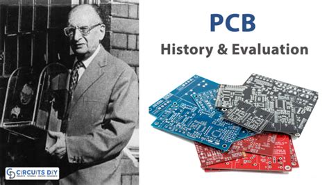
The Birth of the Printed Circuit Board
Paul Eisler and the First Printed Circuit
The true birth of the PCB can be attributed to Paul Eisler, an Austrian engineer who invented the printed circuit while working in England in the 1930s. Eisler’s design involved printing conductive ink onto an insulated substrate, creating a pattern of electrical connections. He used this technique to create a radio set, demonstrating the potential of printed circuits in electronic devices.
World War II and the Advancement of PCB Technology
The outbreak of World War II accelerated the development of PCB technology. The need for compact, reliable, and mass-producible electronic equipment for military applications drove the adoption of printed circuits. In the United States, the National Bureau of Standards (now known as the National Institute of Standards and Technology) began researching printed circuits for military use. By the end of the war, printed circuits had become an integral part of many military electronic systems.

The Evolution of PCB Manufacturing Techniques
The Introduction of Photoengraving
In the 1950s, the process of photoengraving revolutionized PCB manufacturing. This technique involved using a photographic process to transfer the circuit pattern onto a copper-clad substrate. Photoengraving allowed for more precise and detaiLED Circuit patterns, enabling the creation of more complex PCB designs.
The Rise of Multilayer PCBs
As electronic devices became more sophisticated, the need for higher density and more complex circuits grew. This led to the development of multilayer PCBs in the 1960s. Multilayer PCBs consist of multiple layers of conductive material separated by insulating layers, allowing for the routing of a greater number of electrical connections in a smaller space. This innovation paved the way for the miniaturization of electronic devices.
The Advent of Surface Mount Technology (SMT)
In the 1980s, surface mount technology (SMT) emerged as a game-changer in PCB manufacturing. SMT involves mounting components directly onto the surface of the PCB, rather than through holes as in through-hole technology. SMT allowed for smaller components, higher component density, and automated assembly processes, resulting in more compact and cost-effective PCBs.

The Impact of PCBs on Various Industries
Consumer Electronics
The widespread adoption of PCBs has revolutionized the consumer electronics industry. From the earliest radios and televisions to modern smartphones and wearable devices, PCBs have been at the heart of technological advancements. The miniaturization and increased functionality of consumer electronics can be largely attributed to the continuous evolution of PCB technology.
Industrial and Medical Applications
PCBs have found extensive applications in industrial and medical sectors. In industrial settings, PCBs are used in control systems, automation equipment, and power electronics. The reliability and durability of PCBs make them suitable for harsh industrial environments. In the medical field, PCBs are essential components in diagnostic equipment, monitoring devices, and implantable medical devices, enabling advanced healthcare solutions.
Aerospace and Defense
The aerospace and defense industries have been early adopters of PCB technology. PCBs used in these sectors must meet stringent requirements for reliability, durability, and performance under extreme conditions. High-density interconnect (HDI) PCBs and Rigid-flex PCBs have become crucial in aerospace applications, allowing for the integration of complex electronics in limited space and weight constraints.
Modern PCB Design and Manufacturing Trends
High-Density Interconnect (HDI) PCBs
HDI PCBs have emerged as a solution to the increasing demand for miniaturization and high-speed performance. HDI PCBs feature finer lines, smaller vias, and higher component density compared to traditional PCBs. This enables the creation of highly compact and powerful electronic devices, such as smartphones, tablets, and wearables.
Flexible and Rigid-Flex PCBs
Flexible PCBs, made from flexible substrate materials, have gained popularity in recent years. They offer the advantage of conforming to non-planar surfaces and allowing for more creative product designs. Rigid-flex PCBs, which combine rigid and flexible sections, provide the best of both worlds, enabling three-dimensional packaging and improved reliability in applications with limited space.
Sustainable and Eco-Friendly PCB Manufacturing
As environmental concerns have grown, the PCB industry has been focusing on sustainable and eco-friendly manufacturing practices. This includes the use of lead-free materials, the adoption of green manufacturing processes, and the implementation of recycling and waste reduction initiatives. The development of biodegradable and recyclable PCB materials is also an active area of research.
Future Prospects and Challenges
The Internet of Things (IoT) and PCBs
The growth of the Internet of Things (IoT) is driving the demand for PCBs in connected devices. The IoT relies on a vast network of sensors, actuators, and communication modules, all of which require PCBs for their functionality. As the IoT continues to expand, the PCB industry must keep pace with the increasing demand for low-power, wireless-enabled, and highly integrated PCBs.
Advanced Materials and Nanotechnology
The future of PCBs is closely linked to advancements in materials science and nanotechnology. Researchers are exploring the use of advanced materials, such as graphene and carbon nanotubes, to enhance the performance and functionality of PCBs. These materials offer the potential for higher conductivity, lower power consumption, and improved thermal management.
Challenges and Opportunities
The PCB industry faces several challenges, including the need for continuous miniaturization, the demand for higher speeds and bandwidth, and the pressure to reduce costs. Additionally, the increasing complexity of electronic devices requires more sophisticated PCB design and manufacturing techniques. However, these challenges also present opportunities for innovation and growth in the PCB industry.
Frequently Asked Questions (FAQ)
1. What is a printed circuit board (PCB)?
A printed circuit board (PCB) is a flat board made of insulating material with conductive pathways printed or etched onto its surface. It is used to mechanically support and electrically connect electronic components using conductive tracks, pads, and other features.
2. Who invented the printed circuit board?
The invention of the printed circuit board is attributed to Paul Eisler, an Austrian engineer who developed the first printed circuit while working in England in the 1930s.
3. How has PCB technology evolved over time?
PCB technology has evolved significantly since its inception. Key milestones include the introduction of photoengraving in the 1950s, the development of multilayer PCBs in the 1960s, and the adoption of surface mount technology (SMT) in the 1980s. Modern PCB design and manufacturing trends include high-density interconnect (HDI) PCBs, flexible and rigid-flex PCBs, and sustainable manufacturing practices.
4. What role have PCBs played in the growth of various industries?
PCBs have been instrumental in the growth and advancement of various industries, including consumer electronics, industrial and medical applications, and aerospace and defense. They have enabled the miniaturization, increased functionality, and reliability of electronic devices across these sectors.
5. What are some of the future prospects and challenges for the PCB industry?
The future of the PCB industry is closely tied to the growth of the Internet of Things (IoT) and advancements in materials science and nanotechnology. The industry faces challenges such as the need for continuous miniaturization, higher speeds and bandwidth, and cost reduction. However, these challenges also present opportunities for innovation and growth in the PCB industry.
Conclusion
The history of the printed circuit board is a testament to human ingenuity and the relentless pursuit of technological advancement. From its humble beginnings as a concept for simplifying electrical wiring to its current status as an indispensable component in virtually every electronic device, the PCB has undergone a remarkable journey. As we look to the future, the PCB industry will continue to evolve, driven by the demands of emerging technologies and the need for more advanced, efficient, and sustainable solutions. The history of the PCB is not just a story of technological progress; it is a reflection of our ever-growing reliance on electronics and the transformative power of innovation.
| Era | Key Developments |
|---|---|
| Early 20th century | – Advent of electrical circuits – Emergence of circuit diagrams |
| 1930s | – Paul Eisler invents the printed circuit |
| 1940s | – World War II accelerates PCB development for military applications |
| 1950s | – Introduction of photoengraving in PCB manufacturing |
| 1960s | – Development of multilayer PCBs |
| 1980s | – Rise of surface mount technology (SMT) |
| Modern era | – High-density interconnect (HDI) PCBs – Flexible and rigid-flex PCBs – Sustainable and eco-friendly manufacturing practices |
The table above summarizes the key developments in the history of the printed circuit board, highlighting the major milestones and technological advancements that have shaped the PCB industry over the past century.
No responses yet