Introduction to Tenting Via
In the world of printed circuit board (PCB) fabrication, there are many techniques and processes that are crucial for creating high-quality and reliable boards. One such technique is tenting via, which is a method of covering or sealing the Via holes on a PCB during the solder mask application process.
What is a Via?
Before diving into tenting via, it’s important to understand what a via is. A via is a small hole drilled through a PCB that allows electrical connections to be made between different layers of the board. Vias are essential for creating complex circuits that require multiple layers, as they allow signals to travel from one layer to another.
Types of Vias
There are several types of vias used in PCB Fabrication, each with its own specific purpose:
| Via Type | Description |
|---|---|
| Through Hole Via | A hole that goes through all layers of the PCB, allowing components to be mounted on both sides of the board. |
| Blind Via | A hole that starts at an outer layer and ends at an inner layer, but does not go through the entire board. |
| Buried Via | A hole that connects two or more inner layers, but does not extend to the outer layers of the board. |
| Micro Via | A small via with a diameter of 6 mils (0.15mm) or less, used for high-density interconnect (HDI) PCBs. |
The Tenting Via Process
Tenting via is the process of covering via holes with a thin layer of solder mask material during the PCB fabrication process. This is typically done after the copper traces have been etched and before the solder mask is applied to the rest of the board.
Steps in the Tenting Via Process
-
Drilling: The via holes are drilled through the PCB using a specialized drilling machine.
-
Plating: The via holes are plated with a conductive material, typically copper, to create an electrical connection between layers.
-
Solder Mask Application: A thin layer of liquid photoimageable solder mask is applied over the entire surface of the PCB, including the via holes.
-
Exposure and Developing: The solder mask is exposed to UV light through a photomask, which hardens the solder mask in the desired areas. The unexposed areas are then removed using a developing solution, leaving the via holes covered with solder mask.
-
Curing: The PCB is then heated to cure the solder mask, creating a permanent protective layer over the via holes.
Advantages of Tenting Via
Tenting via offers several advantages in PCB fabrication:
-
Protection: Tenting via helps protect the via holes from damage during handling and assembly, as well as from environmental factors such as moisture and dust.
-
Solder Mask Continuity: Tenting via ensures that there is a continuous layer of solder mask over the entire surface of the PCB, which helps prevent short circuits and improves the overall reliability of the board.
-
Improved Aesthetics: Tenting via creates a cleaner and more uniform appearance on the surface of the PCB, as the via holes are not visible through the solder mask.
-
Better Solder Joint Quality: Tenting via can help improve the quality of solder joints by preventing solder from flowing into the via holes during the soldering process.
Disadvantages of Tenting Via
While tenting via offers many benefits, there are also some potential drawbacks to consider:
-
Increased Cost: Tenting via adds an extra step to the PCB fabrication process, which can increase the overall cost of production.
-
Reduced Heat Dissipation: Tenting via can reduce the heat dissipation capabilities of the PCB, as the solder mask material acts as an insulator and can trap heat inside the via holes.
-
Potential for Trapped Air: If the tenting via process is not performed correctly, there is a risk of trapping air bubbles inside the via holes, which can lead to reliability issues over time.

Alternatives to Tenting Via
While tenting via is a common technique used in PCB fabrication, there are some alternatives that may be more suitable for certain applications:
Via Plugging
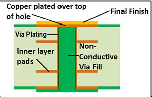
Via plugging is a process where the via holes are filled with a non-conductive material, such as epoxy or resin, before the solder mask is applied. This creates a completely smooth surface on the PCB and eliminates the need for tenting via.
Via Capping
Via capping is a process where a thin layer of copper is plated over the top of the via holes, creating a “cap” that seals the hole and protects it from damage. This technique is often used in high-reliability applications where the via holes need to be completely sealed.
Via in Pad
Via in pad is a technique where the via holes are placed directly in the solder pad of a component, rather than in a separate location on the PCB. This allows for more efficient use of space on the board and can improve the signal integrity of the circuit.

Frequently Asked Questions (FAQ)
-
Q: Is tenting via necessary for all PCBs?
A: No, tenting via is not necessary for all PCBs. It is typically used in applications where the via holes need to be protected from damage or where a smooth, uniform surface is desired. -
Q: Can tenting via be done selectively on a PCB?
A: Yes, tenting via can be done selectively on a PCB. This means that only certain via holes are covered with solder mask, while others are left exposed. -
Q: How does tenting via affect the electrical properties of a PCB?
A: Tenting via can have a slight impact on the electrical properties of a PCB, as the solder mask material acts as an insulator and can affect the impedance of the circuit. However, this effect is typically negligible and can be accounted for during the design process. -
Q: Is it possible to remove tenting via from a PCB after it has been applied?
A: Yes, it is possible to remove tenting via from a PCB using a process called “via stripping”. This involves using a chemical solution to dissolve the solder mask material covering the via holes. -
Q: Can tenting via be used with any type of solder mask?
A: Tenting via can be used with most types of solder mask, including liquid photoimageable (LPI) and dry film solder mask. However, the specific process and parameters may vary depending on the type of solder mask being used.

Conclusion
Tenting via is an important technique used in PCB fabrication to protect via holes and create a smooth, uniform surface on the board. By covering the via holes with a thin layer of solder mask, tenting via helps improve the reliability, aesthetics, and solder joint quality of the PCB.
While tenting via offers many benefits, it is not necessary for all applications and there are some potential drawbacks to consider, such as increased cost and reduced heat dissipation. Alternatives to tenting via, such as via plugging, via capping, and via in pad, may be more suitable for certain applications.
Overall, tenting via is a valuable tool in the PCB fabrication process that can help ensure the quality and reliability of the final product. By understanding the advantages and limitations of this technique, PCB Designers and manufacturers can make informed decisions about when and how to use tenting via in their projects.
No responses yet