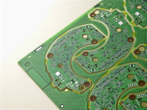
What is an HDI PCB?
An HDI PCB is a type of printed circuit board that features higher wiring density and smaller vias than traditional PCBs. This is achieved through the use of advanced manufacturing techniques, such as microvias, buried vias, and sequential lamination. HDI PCBs allow for more complex routing and component placement, enabling designers to create highly compact and efficient electronic devices.
Key Features of HDI PCBs
- High Wiring Density
- Smaller Vias
- Microvias
- Buried Vias
- Sequential Lamination
Benefits of Using HDI PCBs
Space Savings
One of the primary benefits of using HDI PCBs is the significant space savings they offer. By utilizing smaller vias and higher wiring density, designers can create more compact layouts, reducing the overall size of the PCB. This is particularly important for applications where space is limited, such as smartphones, wearables, and IoT devices.
Improved Signal Integrity
HDI PCBs offer improved signal integrity compared to traditional PCBs. The shorter signal paths and reduced layer count minimize signal loss and crosstalk, resulting in better overall performance. This is crucial for high-speed applications, such as 5G networks, where signal integrity is paramount.
Enhanced Thermal Management
The compact nature of HDI PCBs allows for better thermal management. With components placed closer together, heat dissipation becomes more efficient, reducing the risk of thermal-related failures. Additionally, the use of advanced materials, such as metal-core substrates, can further enhance thermal performance.
Cost-Effectiveness
While HDI PCBs may have a higher initial cost compared to traditional PCBs, they can be more cost-effective in the long run. The space savings and improved performance offered by HDI PCBs can lead to reduced overall system costs, as fewer components and materials may be required. Furthermore, the increased reliability and longer lifespan of HDI PCBs can result in lower maintenance and replacement costs.

Applications of HDI PCBs
HDI PCBs find applications in a wide range of industries, including:
- Consumer Electronics
- Smartphones
- Tablets
- Wearables
-
Digital Cameras
-
Automotive
- Advanced Driver Assistance Systems (ADAS)
- Infotainment Systems
-
Engine Control Units (ECUs)
-
Medical Devices
- Implantable Devices
- Diagnostic Equipment
-
Wearable Health Monitors
-
Aerospace and Defense
- Avionics
- Radar Systems
-
Satellite Communication
-
Industrial Automation
- Robotics
- Process Control Systems
- Industrial IoT Devices

HDI PCB Design Considerations
When designing an HDI PCB, several factors must be taken into account to ensure optimal performance and manufacturability. Some key considerations include:
Layer Stack-up
The layer stack-up of an HDI PCB is crucial for achieving the desired electrical performance and signal integrity. Designers must carefully select the number of layers, material properties, and via structures to meet the specific requirements of the application.
Via Types and Sizes
HDI PCBs utilize various types of vias, such as microvias, buried vias, and blind vias, to achieve higher wiring density and more compact layouts. Designers must choose the appropriate via types and sizes based on the design requirements, manufacturing capabilities, and cost constraints.
Material Selection
The choice of materials for an HDI PCB is critical for ensuring reliability and performance. Factors such as dielectric constant, loss tangent, thermal conductivity, and mechanical strength must be considered when selecting the substrate and laminate materials.
Design for Manufacturability (DFM)
To ensure the successful fabrication of an HDI PCB, designers must adhere to DFM guidelines. This includes considering aspects such as minimum trace widths, clearances, via sizes, and pad sizes. Collaborating closely with the PCB manufacturer can help optimize the design for manufacturability and minimize potential issues.

HDI PCB Manufacturing Process
The manufacturing process for HDI PCBs is more complex than that of traditional PCBs due to the advanced techniques and materials involved. The process typically includes the following steps:
- Design and Artwork Creation
- Material Selection and Preparation
- Drilling and Plating
- Patterning and Etching
- Lamination and Pressing
- Solder Mask Application
- Surface Finish Application
- Electrical Testing and Inspection
Each step requires precise control and adherence to stringent quality standards to ensure the final product meets the desired specifications and performance requirements.
Choosing the Right HDI PCB Manufacturer
Selecting the right HDI PCB manufacturer is essential for ensuring the success of your project. When evaluating potential manufacturers, consider the following factors:
- Experience and Expertise
- Manufacturing Capabilities and Equipment
- Quality Control and Certifications
- Lead Time and Delivery
- Customer Support and Communication
- Cost and Value for Money
A reputable HDI PCB manufacturer will have a proven track record of delivering high-quality products, provide responsive customer support, and offer competitive pricing without compromising on quality.
FAQs
-
Q: What is the minimum feature size achievable with HDI PCBs?
A: HDI PCBs can achieve minimum feature sizes as small as 50 microns (0.05 mm) for traces and spaces, and 100 microns (0.1 mm) for via diameters. -
Q: Are HDI PCBs more expensive than traditional PCBs?
A: Yes, HDI PCBs typically have a higher initial cost compared to traditional PCBs due to the advanced materials and manufacturing techniques involved. However, they can be more cost-effective in the long run due to space savings, improved performance, and increased reliability. -
Q: Can HDI PCBs be used for high-power applications?
A: HDI PCBs are primarily designed for high-density, low-power applications. While they can be used in some high-power applications with proper design considerations, they may not always be the most suitable choice. Traditional PCBs with thicker copper layers and larger trace widths are often better suited for high-power applications. -
Q: What are the typical layer counts for HDI PCBs?
A: HDI PCBs typically have layer counts ranging from 4 to 16 layers, depending on the complexity of the design and the application requirements. Higher layer counts allow for more complex routing and better signal integrity but also increase the cost and manufacturing complexity. -
Q: How long does it take to manufacture an HDI PCB?
A: The lead time for manufacturing an HDI PCB can vary depending on the complexity of the design, the chosen manufacturer, and the order quantity. Typical lead times range from 2 to 4 weeks, but expedited services may be available for urgent projects.
Conclusion
HDI PCBs offer numerous benefits, including space savings, improved signal integrity, enhanced thermal management, and cost-effectiveness. They find applications in a wide range of industries, from consumer electronics to aerospace and defense. When considering whether HDI PCBs can meet your needs, it is essential to evaluate your specific requirements, design considerations, and manufacturing constraints.
Choosing the right HDI PCB manufacturer is crucial for ensuring the success of your project. By partnering with an experienced and reputable manufacturer, you can leverage their expertise to optimize your design, minimize potential issues, and achieve the desired performance and reliability.
As technology continues to advance, the demand for HDI PCBs is expected to grow, driven by the need for more compact, efficient, and high-performance electronic devices. By understanding the capabilities and limitations of HDI PCBs, you can make informed decisions and stay ahead of the curve in this rapidly evolving industry.
No responses yet