Introduction to Solder Mask
Solder mask, also known as solder resist or solder stop mask, is a thin lacquer-like layer of polymer applied to the copper traces of a printed circuit board (PCB). Its primary purpose is to prevent solder from bridging between conductors, thereby preventing short circuits. Solder mask also provides protection against oxidation and contamination of the copper traces, improving the durability and reliability of the PCB.
Key Functions of Solder Mask
- Insulation: Solder mask acts as an insulating layer, preventing accidental electrical contact between components and traces.
- Solder Control: It prevents solder from flowing beyond the desired areas during the soldering process, ensuring precise solder connections.
- Protection: Solder mask shields the copper traces from oxidation, corrosion, and other environmental factors that can degrade the PCB’s performance.
- Aesthetics: It provides a uniform appearance to the PCB, with green being the most common color, although other colors like red, blue, and black are also available.
Composition and Application of Solder Mask
Materials Used in Solder Mask
Solder mask is typically composed of a photosensitive polymer, such as:
- Epoxy: Known for its excellent adhesion, chemical resistance, and durability.
- Acrylic: Offers good electrical insulation and flexibility.
- Polyurethane: Provides high resistance to abrasion and chemicals.
- Polyimide: Suitable for high-temperature applications due to its thermal stability.
These polymers are mixed with fillers, pigments, and other additives to achieve the desired properties and color.
Solder Mask Application Process
The application of solder mask involves several steps:
- Cleaning: The PCB surface is cleaned to remove any contaminants or debris.
- Solder Mask Application: The liquid solder mask is applied to the PCB surface using screen printing, spray coating, or curtain coating methods.
- Pre-baking: The coated PCB is heated to partially cure the solder mask and remove any solvents.
- Exposure: The solder mask is exposed to UV light through a photomask, which hardens the exposed areas while leaving the unexposed areas soluble.
- Developing: The unexposed areas are removed using a chemical developer, revealing the copper pads and traces that require soldering.
- Final Curing: The PCB is heated to fully cure the solder mask, making it durable and resistant to environmental factors.
| Step | Process | Purpose |
|---|---|---|
| 1 | Cleaning | Remove contaminants and debris |
| 2 | Solder Mask Application | Apply liquid solder mask to PCB surface |
| 3 | Pre-baking | Partially cure solder mask and remove solvents |
| 4 | Exposure | Harden exposed areas using UV light |
| 5 | Developing | Remove unexposed areas to reveal copper pads and traces |
| 6 | Final Curing | Fully cure solder mask for durability and resistance |

Solder Mask Properties and Performance
Electrical Properties
Solder mask plays a crucial role in maintaining the electrical integrity of a PCB. Its key electrical properties include:
- Dielectric Strength: The ability to withstand high voltage without breaking down, typically measured in volts per mil (V/mil).
- Insulation Resistance: The resistance to electrical current leakage between conductors, measured in ohms (Ω).
- Dielectric Constant: The ratio of the permittivity of the solder mask to that of a vacuum, which affects the signal propagation speed and impedance.
- Dissipation Factor: A measure of the power loss in the solder mask due to dielectric heating, expressed as a ratio of the power lost to the power stored.
Mechanical Properties
Solder mask must also possess good mechanical properties to protect the PCB from physical damage and ensure long-term reliability. Important mechanical properties include:
- Adhesion: The ability to adhere strongly to the copper surface and resist delamination.
- Hardness: Resistance to scratching, abrasion, and indentation.
- Flexibility: The ability to withstand bending and thermal expansion without cracking or peeling.
- Tensile Strength: The maximum stress the solder mask can withstand before breaking.
Chemical Resistance
Solder mask must be resistant to various chemicals encountered during PCB manufacturing, assembly, and operation. These include:
- Fluxes: Used during soldering to remove oxides and promote wetting of the solder.
- Cleaning Agents: Used to remove flux residues and other contaminants after soldering.
- Solvents: Used in various cleaning and coating processes.
- Oils and Greases: Used for lubrication and protection of mechanical components.
Thermal Properties
Solder mask must withstand the high temperatures encountered during soldering and operation without degrading or losing its properties. Key thermal properties include:
- Glass Transition Temperature (Tg): The temperature at which the solder mask transitions from a hard, glassy state to a soft, rubbery state.
- Coefficient of Thermal Expansion (CTE): The rate at which the solder mask expands with increasing temperature, which should be close to that of the PCB substrate to minimize stress.
- Thermal Decomposition Temperature: The temperature at which the solder mask begins to break down and lose its properties.

Solder Mask Design Considerations
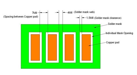
Solder Mask Clearance
Solder mask clearance refers to the space between the edge of the copper pad and the opening in the solder mask. Proper clearance is essential to ensure good solder joint formation and prevent solder mask from interfering with the soldering process. Factors affecting solder mask clearance include:
- Copper Pad Size: Larger pads require greater clearance to accommodate the solder volume.
- Solder Mask Thickness: Thicker solder mask requires larger clearances to prevent bridging.
- Solder Mask Registration: Misalignment between the solder mask and copper layers can reduce the effective clearance.
Typical solder mask clearances range from 0.05 mm to 0.2 mm, depending on the PCB design rules and manufacturing capabilities.
Solder Mask Sliver
Solder mask sliver refers to the narrow strip of solder mask between two closely spaced copper features, such as pads or traces. If the sliver is too narrow, it may break off during manufacturing or operation, causing short circuits or other defects. To prevent this, PCB designers must adhere to minimum solder mask sliver width rules, which typically range from 0.1 mm to 0.15 mm, depending on the PCB fabricator’s capabilities.
Solder Mask Color and Markings
While green is the most common solder mask color, other colors like red, blue, black, and white are also available. The choice of color can be based on aesthetic preferences, functional requirements, or industry standards. For example:
- Black solder mask is often used for high-end consumer electronics to provide a sleek, modern appearance.
- White solder mask is used in LED lighting applications to maximize light reflection and improve efficiency.
- Red or blue solder mask may be used to visually distinguish different PCB assemblies or versions.
In addition to color, solder mask can also include markings such as component outlines, polarity indicators, and text labels to assist in PCB Assembly and troubleshooting. These markings are typically applied using silk screen printing or direct legend ink.

Solder Mask Quality Control and Inspection
Solder Mask Defects
Various defects can occur during the solder mask application process, affecting the quality and reliability of the PCB. Common solder mask defects include:
- Pinholes: Small holes in the solder mask that expose the underlying copper, causing potential short circuits or corrosion.
- Blistering: Localized delamination of the solder mask from the copper surface, often due to improper curing or contamination.
- Peeling: Separation of the solder mask from the copper surface along the edges of pads or traces, usually caused by poor adhesion or mechanical stress.
- Misregistration: Misalignment between the solder mask and copper layers, resulting in exposed copper or reduced clearances.
- Contamination: Presence of foreign particles or residues on the solder mask surface, which can interfere with soldering or cause reliability issues.
Inspection Methods
To ensure the quality of the solder mask and detect any defects, various inspection methods are employed during PCB manufacturing. These include:
- Visual Inspection: Manual or automated optical inspection of the PCB surface for visible defects such as pinholes, blistering, or peeling.
- Microscopic Inspection: Use of high-magnification microscopes to examine the solder mask surface and edge definition for smaller defects.
- Thickness Measurement: Use of non-contact methods such as laser triangulation or white light interferometry to measure the thickness of the solder mask layer.
- Adhesion Testing: Destructive tests such as cross-hatch or tape pull tests to evaluate the adhesion of the solder mask to the copper surface.
- Electrical Testing: Resistance and insulation testing to verify the electrical properties of the solder mask and detect any short circuits or leakage paths.
By implementing strict quality control measures and inspection procedures, PCB manufacturers can ensure that the solder mask meets the specified requirements and provides reliable protection for the PCB throughout its lifecycle.
Frequently Asked Questions (FAQ)
- What is the primary purpose of solder mask on a PCB?
-
The primary purpose of solder mask is to prevent solder bridging between conductors and protect the copper traces from oxidation and contamination.
-
What are the most common materials used in solder mask?
-
The most common materials used in solder mask are photosensitive polymers such as epoxy, acrylic, polyurethane, and polyimide.
-
What is the typical thickness of a solder mask layer?
-
The typical thickness of a solder mask layer ranges from 0.01 mm to 0.03 mm (10 to 30 microns).
-
How does solder mask color affect PCB functionality?
-
Solder mask color generally does not affect PCB functionality, but certain colors may be chosen for specific applications, such as white for LED lighting or black for high-end consumer electronics.
-
What are the most common defects that can occur in solder mask?
- The most common defects that can occur in solder mask include pinholes, blistering, peeling, misregistration, and contamination.
Conclusion
Solder mask is an essential component of modern PCBs, providing critical protection against solder bridging, oxidation, and contamination. Its electrical, mechanical, chemical, and thermal properties play a vital role in ensuring the reliability and longevity of electronic devices. By understanding the composition, application process, design considerations, and quality control aspects of solder mask, PCB designers and manufacturers can create high-quality, resilient circuit boards that meet the demands of today’s increasingly complex electronic systems. As technology continues to advance, the development of new solder mask materials and processes will be crucial in enabling the next generation of PCBs and electronic devices.
No responses yet