Introduction to Vias and Their Importance in PCB Design
In the world of printed circuit board (PCB) design, vias play a crucial role in connecting different layers of the board, allowing for more complex and compact designs. Vias are essentially small holes drilled through the PCB, which are then plated with a conductive material to create an electrical connection between layers. There are several types of vias, each with its own unique characteristics and applications. In this article, we will focus on three specific types of vias: tenting vias, plugged vias, and via in pad.
What are Tenting Vias?
Tenting vias, also known as covered vias or mask-covered vias, are a type of via where the solder mask is applied over the Via hole, creating a thin, insulating layer. This process is called Via tenting because the solder mask forms a “tent” over the via hole. Tenting vias offer several advantages over other types of vias, which we will discuss in detail later in this article.
What are Plugged Vias?
Plugged vias, also referred to as filled vias or Via Filling, are vias that have been completely filled with a non-conductive material, such as epoxy or resin. This process is done to create a smooth, flat surface on the PCB, which is essential for certain applications, such as high-density interconnect (HDI) PCBs or PCBs that require a specific impedance control.
What is Via in Pad?
Via in pad, as the name suggests, is a design technique where a via is placed directly on a component pad. This approach is often used in high-density PCB designs to save space and improve signal integrity. By placing the via directly on the pad, designers can eliminate the need for additional traces, which can help reduce the overall size of the PCB.
Advantages of Tenting Vias
1. Improved Solder Mask Coverage
One of the primary advantages of tenting vias is that it provides better solder mask coverage compared to non-tented vias. When a via is tented, the solder mask forms a thin, protective layer over the via hole, which helps prevent solder from flowing into the via during the soldering process. This is particularly important for surface mount technology (SMT) components, as it helps ensure a proper solder joint between the component and the pad.
2. Enhanced Electrical Insulation
Tenting vias also provides enhanced electrical insulation between the via and the surrounding components or traces. The solder mask acts as an insulating layer, reducing the risk of short circuits or other electrical issues that can arise when conductive materials come into contact with exposed vias.
3. Improved Mechanical Strength
Another benefit of tenting vias is that it can improve the mechanical strength of the PCB. When a via is tented, the solder mask helps to reinforce the via, making it more resistant to mechanical stress and vibration. This can be particularly important in applications where the PCB is subjected to harsh environmental conditions or high levels of physical stress.
4. Reduced Risk of Contamination
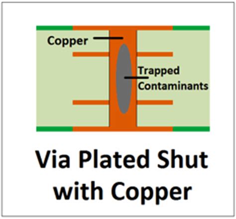
Tenting vias can also help reduce the risk of contamination in the via hole. In non-tented vias, the exposed hole can act as a trap for dirt, dust, and other contaminants, which can lead to reliability issues over time. By covering the via hole with solder mask, tenting helps prevent these contaminants from entering the via, thus improving the overall reliability of the PCB.

Advantages of Plugged Vias
1. Improved Signal Integrity
One of the main advantages of plugged vias is that they can help improve signal integrity in high-speed PCB designs. When a via is left unfilled, it can create a discontinuity in the signal path, leading to reflections and other signal integrity issues. By filling the via with a non-conductive material, designers can create a more uniform signal path, reducing the risk of signal degradation.
2. Enhanced Thermal Management
Plugged vias can also help improve thermal management in PCBs. When a via is filled with a thermally conductive material, such as a thermal epoxy, it can help dissipate heat more efficiently from the components on the PCB. This can be particularly important in high-power applications, where effective thermal management is critical to ensure reliable operation and prevent component failure.
3. Increased Mechanical Strength
Similar to tenting vias, plugged vias can also improve the mechanical strength of the PCB. When a via is filled with a solid material, it becomes more resistant to mechanical stress and vibration, which can help prevent damage to the PCB over time. This can be especially important in applications where the PCB is subjected to harsh environmental conditions or high levels of physical stress.
4. Improved Plating Uniformity
Plugged vias can also help improve the uniformity of the plating process in the via hole. In non-plugged vias, the plating process can sometimes result in uneven coverage, leading to variations in the electrical and mechanical properties of the via. By filling the via with a solid material before plating, designers can create a more uniform surface for the plating process, resulting in more consistent via properties across the PCB.

Advantages of Via in Pad
1. Space Savings
One of the primary advantages of via in pad is that it can help save space on the PCB. By placing the via directly on the component pad, designers can eliminate the need for additional traces, which can help reduce the overall size of the PCB. This can be particularly important in high-density designs, where space is at a premium.
2. Improved Signal Integrity
Via in pad can also help improve signal integrity in high-speed PCB designs. By placing the via directly on the pad, designers can minimize the length of the signal path, reducing the risk of signal degradation due to impedance mismatches or other factors. This can help ensure more reliable high-speed performance, particularly in applications such as high-frequency RF designs.
3. Enhanced Thermal Management
Similar to plugged vias, via in pad can also help improve thermal management in PCBs. By placing the via directly on the pad, designers can create a more direct thermal path from the component to the via, allowing for more efficient heat dissipation. This can be particularly important in high-power applications, where effective thermal management is critical to ensure reliable operation and prevent component failure.
4. Reduced Manufacturing Costs
Via in pad can also help reduce manufacturing costs in some cases. By eliminating the need for additional traces and reducing the overall size of the PCB, via in pad can help simplify the manufacturing process and reduce the amount of material required. This can lead to lower production costs, particularly in high-volume applications.

Comparing Tenting Vias, Plugged Vias, and Via in Pad
| Characteristic | Tenting Vias | Plugged Vias | Via in Pad |
|---|---|---|---|
| Solder Mask Coverage | Improved | N/A | N/A |
| Electrical Insulation | Enhanced | N/A | N/A |
| Mechanical Strength | Improved | Increased | N/A |
| Contamination Risk | Reduced | N/A | N/A |
| Signal Integrity | N/A | Improved | Improved |
| Thermal Management | N/A | Enhanced | Enhanced |
| Plating Uniformity | N/A | Improved | N/A |
| Space Savings | N/A | N/A | Yes |
| Manufacturing Costs | N/A | N/A | Reduced |
As shown in the table above, each type of via has its own unique advantages and characteristics. Tenting vias are particularly useful for improving solder mask coverage, enhancing electrical insulation, and reducing the risk of contamination. Plugged vias, on the other hand, are well-suited for improving signal integrity, thermal management, and plating uniformity. Finally, via in pad is an excellent choice for saving space on the PCB, improving signal integrity, and enhancing thermal management.
Choosing the Right Via Type for Your PCB Design
When deciding which type of via to use in your PCB design, there are several factors to consider. These include:
- The specific requirements of your application (e.g., high-speed, high-power, high-density)
- The available space on the PCB
- The desired level of signal integrity and thermal management
- The manufacturing capabilities of your PCB fabricator
- The overall cost and complexity of the design
By carefully evaluating these factors and consulting with your PCB fabricator, you can select the via type that best meets the needs of your specific application.
Frequently Asked Questions (FAQ)
-
Q: What is the difference between tenting vias and plugged vias?
A: Tenting vias involve applying a thin layer of solder mask over the via hole, while plugged vias are completely filled with a non-conductive material, such as epoxy or resin. -
Q: Can via in pad be used with surface mount components?
A: Yes, via in pad can be used with surface mount components, and it is often used in high-density designs to save space on the PCB. -
Q: Are there any disadvantages to using plugged vias?
A: One potential disadvantage of plugged vias is that they can add complexity and cost to the manufacturing process, as the via filling process requires additional steps and materials. -
Q: Can tenting vias be used in high-speed PCB designs?
A: While tenting vias can provide enhanced electrical insulation and improved solder mask coverage, they may not be the best choice for high-speed designs where signal integrity is a primary concern. In these cases, plugged vias or via in pad may be more appropriate. -
Q: How do I choose the right via type for my PCB design?
A: Choosing the right via type depends on several factors, including the specific requirements of your application, the available space on the PCB, the desired level of signal integrity and thermal management, the manufacturing capabilities of your PCB fabricator, and the overall cost and complexity of the design. It is essential to carefully evaluate these factors and consult with your PCB fabricator to select the via type that best meets your needs.
Conclusion
Tenting vias, plugged vias, and via in pad are all valuable techniques in PCB design, each with its own unique advantages and characteristics. By understanding the benefits and limitations of each via type, designers can make informed decisions about which approach to use in their specific applications.
Tenting vias are particularly useful for improving solder mask coverage, enhancing electrical insulation, and reducing the risk of contamination. Plugged vias, on the other hand, are well-suited for improving signal integrity, thermal management, and plating uniformity. Finally, via in pad is an excellent choice for saving space on the PCB, improving signal integrity, and enhancing thermal management.
Ultimately, the key to successful PCB design is to carefully evaluate the specific requirements of your application and work closely with your PCB fabricator to select the via type that best meets your needs. By doing so, you can create PCBs that are reliable, high-performing, and cost-effective, regardless of the complexity or challenges of your design.
No responses yet