What are Thick Copper PCBs?
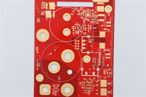
Thick Copper PCBs are a type of printed circuit board that features copper layers with a thickness greater than the standard 1 oz. (35 µm) used in most PCBs. The copper thickness can range from 2 oz. (70 µm) to 20 oz. (700 µm) or even more in some cases. These PCBs are designed to handle high currents, provide better heat dissipation, and offer improved mechanical stability compared to standard PCBs.
Characteristics of Thick Copper PCBs
Copper Thickness
The defining characteristic of thick copper PCBs is the increased thickness of the copper layers. The table below shows the common copper thicknesses used in thick copper PCBs:
| Copper Weight (oz.) | Thickness (µm) |
|---|---|
| 2 | 70 |
| 3 | 105 |
| 4 | 140 |
| 6 | 210 |
| 8 | 280 |
| 10 | 350 |
| 12 | 420 |
| 20 | 700 |
The choice of copper thickness depends on the specific requirements of the application, such as current carrying capacity, heat dissipation needs, and mechanical stability.
Current Carrying Capacity
One of the primary advantages of thick copper PCBs is their ability to handle high currents. The increased copper thickness allows for better current flow and reduces resistance, minimizing voltage drops and power losses. This makes thick copper PCBs ideal for power electronics applications, such as power supplies, motor drives, and high-current circuitry.
Heat Dissipation
Thick copper PCBs offer improved heat dissipation compared to standard PCBs. The increased copper thickness provides a larger cross-sectional area for heat conduction, allowing heat to be efficiently transferred away from critical components. This helps in maintaining stable operating temperatures, enhancing reliability, and preventing thermal damage to sensitive components.
Mechanical Stability
The increased copper thickness in thick copper PCBs also contributes to improved mechanical stability. Thicker copper layers provide better rigidity and resistance to warping, twisting, and bending. This is particularly important in applications where the PCB is subjected to mechanical stress, vibrations, or harsh environmental conditions.
Manufacturing Process of Thick Copper PCBs
The manufacturing process of thick copper PCBs is similar to that of standard PCBs, with a few additional steps to accommodate the increased copper thickness.
Substrate Preparation
The process begins with the preparation of the substrate material, typically FR-4 or other high-quality dielectric materials. The substrate is cleaned, and any necessary pre-treatment is applied to ensure proper adhesion of the copper layers.
Copper Deposition
The next step involves the deposition of thick copper layers onto the substrate. This can be achieved through various methods, such as electroplating, direct bonding, or foil lamination. The choice of method depends on the desired copper thickness, the size of the PCB, and the manufacturing capabilities of the PCB fabricator.
Patterning and Etching
Once the thick copper layers are deposited, the PCB undergoes the patterning and etching process. The desired circuit layout is transferred onto the copper layers using photolithography or other imaging techniques. The unwanted copper areas are then etched away, leaving behind the desired circuit pattern.
Drilling and Plating
After patterning and etching, the PCB is drilled to create the necessary holes for component mounting and inter-layer connections. The holes are then plated with copper to establish electrical connectivity between layers.
Solder Mask and Silkscreen
A solder mask layer is applied to the PCB to protect the copper traces from oxidation and prevent short circuits during soldering. The silkscreen layer is then added to provide component labels, markings, and other visual indicators.
Surface Finish
Finally, the PCB undergoes a surface finish process to enhance solderability, protect the exposed copper, and improve the overall appearance. Common surface finishes for thick copper PCBs include Hot Air Solder Leveling (HASL), Electroless Nickel Immersion Gold (ENIG), and Organic Solderability Preservative (OSP).

Advantages of Thick Copper PCBs
Thick copper PCBs offer several advantages over standard PCBs, making them suitable for a wide range of applications.
High Current Carrying Capacity
The increased copper thickness in thick copper PCBs allows for higher current carrying capacity compared to standard PCBs. This makes them ideal for power electronics applications, where high currents need to be efficiently handled without causing excessive voltage drops or power losses.
Improved Heat Dissipation
Thick copper PCBs provide better heat dissipation due to the increased copper cross-sectional area. The enhanced thermal conductivity helps in dissipating heat generated by components, reducing thermal stress and improving overall system reliability.
Enhanced Mechanical Stability
The thicker copper layers in thick copper PCBs offer improved mechanical stability, making them more resistant to warping, twisting, and bending. This is particularly beneficial in applications where the PCB is subjected to mechanical stress or vibrations, such as in automotive, aerospace, or industrial environments.
Reduced Electromagnetic Interference (EMI)
Thick copper PCBs can help in reducing electromagnetic interference (EMI) by providing better shielding and grounding. The increased copper thickness acts as a barrier against electromagnetic radiation, minimizing crosstalk and interference between different circuit sections.
Longer Lifespan
The robust construction and improved thermal management of thick copper PCBs contribute to a longer lifespan compared to standard PCBs. The increased copper thickness helps in withstanding thermal cycling, mechanical stress, and other environmental factors, resulting in improved reliability and durability.
Applications of Thick Copper PCBs
Thick copper PCBs find applications in various industries and domains where high current handling, efficient heat dissipation, and mechanical stability are critical. Some common applications include:
-
Power Electronics: Thick copper PCBs are extensively used in power electronics applications, such as power supplies, motor drives, inverters, and converters. The high current carrying capacity and improved heat dissipation make them suitable for handling high power densities.
-
Automotive Electronics: In the automotive industry, thick copper PCBs are used in applications such as engine control units (ECUs), power distribution modules, and battery management systems. The enhanced mechanical stability and thermal management capabilities make them well-suited for the demanding automotive environment.
-
Industrial Automation: Thick copper PCBs are employed in industrial automation systems, including motor controllers, sensors, and actuators. The improved current handling and heat dissipation properties ensure reliable operation in harsh industrial conditions.
-
LED Lighting: High-power LED lighting applications often utilize thick copper PCBs to manage the high currents and heat generated by the LEDs. The efficient heat dissipation provided by thick copper layers helps in maintaining optimal LED performance and longevity.
-
Aerospace and Defense: Thick copper PCBs are used in aerospace and defense applications, where reliability, mechanical stability, and thermal management are critical. They are employed in avionics systems, radar modules, and communication equipment.
-
Medical Equipment: Medical devices, such as imaging systems, surgical instruments, and monitoring equipment, often utilize thick copper PCBs for their high current handling capabilities and improved EMI shielding. The enhanced reliability and durability ensure safe and accurate operation in medical settings.
Frequently Asked Questions (FAQ)
-
What is the difference between thick copper PCBs and standard PCBs?
Thick copper PCBs have copper layers with a thickness greater than the standard 1 oz. (35 µm) used in most PCBs. The increased copper thickness provides higher current carrying capacity, improved heat dissipation, and enhanced mechanical stability compared to standard PCBs. -
What are the common copper thicknesses used in thick copper PCBs?
Common copper thicknesses used in thick copper PCBs range from 2 oz. (70 µm) to 20 oz. (700 µm) or more. The choice of copper thickness depends on the specific requirements of the application, such as current carrying capacity, heat dissipation needs, and mechanical stability. -
How do thick copper PCBs handle high currents?
The increased copper thickness in thick copper PCBs allows for better current flow and reduces resistance, minimizing voltage drops and power losses. This enables them to handle high currents efficiently, making them suitable for power electronics applications. -
What are the advantages of using thick copper PCBs?
Thick copper PCBs offer several advantages, including high current carrying capacity, improved heat dissipation, enhanced mechanical stability, reduced electromagnetic interference (EMI), and longer lifespan compared to standard PCBs. -
In which industries are thick copper PCBs commonly used?
Thick copper PCBs find applications in various industries, including power electronics, automotive electronics, industrial automation, LED lighting, aerospace and defense, and medical equipment. They are used in applications where high current handling, efficient heat dissipation, and mechanical stability are critical.
Conclusion
Thick copper PCBs have emerged as a valuable solution for applications demanding high current handling, efficient heat dissipation, and enhanced mechanical stability. With their increased copper thickness, these PCBs offer numerous advantages over standard PCBs, making them suitable for a wide range of industries and applications.
As technology continues to advance and the demand for reliable and high-performance electronic systems grows, thick copper PCBs are expected to play an increasingly important role in shaping the future of electronics. By understanding the characteristics, manufacturing processes, and applications of thick copper PCBs, designers and engineers can leverage their benefits to develop robust and efficient electronic solutions.

No responses yet