Introduction to PCB Soldering
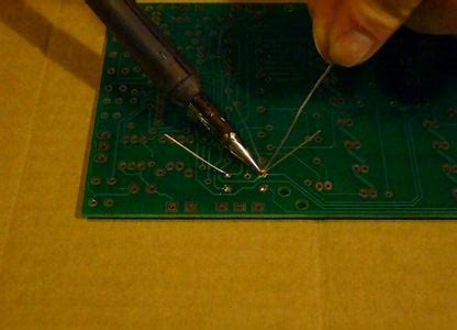
Printed Circuit Board (PCB) soldering is a crucial step in the assembly of electronic devices. It involves the process of joining electronic components to the PCB using a molten metal alloy called solder. Proper soldering ensures reliable electrical connections and the overall functionality of the device. However, several problems can arise during the PCB soldering process, which can lead to issues such as poor connections, short circuits, and even component damage.
When designing a PCB layout for soldering, it is essential to pay attention to various factors to minimize the risk of soldering problems. This article will discuss the key problems that should be considered when drawing a PCB for soldering and provide tips on how to optimize the design for better soldering results.
Key Problems in PCB Soldering
1. Pad Size and Spacing
One of the primary concerns when designing a PCB for soldering is the size and spacing of the component pads. If the pads are too small, it becomes difficult for the soldering iron to make proper contact, leading to weak or incomplete solder joints. On the other hand, if the pads are too large, it can result in excessive solder usage and increased the risk of bridging between adjacent pads.
To address this problem, it is crucial to follow the recommended pad sizes and spacing guidelines provided by the component manufacturers. The following table shows some general guidelines for pad sizes based on component package types:
| Component Package | Recommended Pad Size (mm) |
|---|---|
| 0402 | 0.5 x 0.5 |
| 0603 | 0.8 x 0.8 |
| 0805 | 1.0 x 1.0 |
| 1206 | 1.5 x 1.5 |
| SOIC-8 | 0.6 x 2.2 |
| TQFP-32 | 0.4 x 0.8 |
It is also important to maintain adequate spacing between pads to prevent solder bridging. A minimum spacing of 0.2mm to 0.5mm is generally recommended, depending on the component size and soldering method used.
2. Thermal Relief
During the soldering process, heat is applied to the component pads to melt the solder and create a connection. However, if the PCB has large copper areas, such as ground planes or power planes, the heat can dissipate quickly, making it difficult to achieve proper solder joint formation.
To mitigate this issue, thermal relief patterns should be incorporated into the PCB design. Thermal relief is a design technique that involves creating small copper traces or spokes that connect the component pad to the larger copper area. These traces act as thermal barriers, allowing the heat to concentrate on the pad during soldering.
Some common thermal relief patterns include:
- Four-spoke thermal relief
- Six-spoke thermal relief
- Direct connection with reduced copper area
The choice of thermal relief pattern depends on factors such as the component size, copper area size, and soldering method used.
3. Solder Mask Clearance
Solder mask is a protective layer applied to the PCB surface to prevent solder from adhering to unwanted areas. It also helps to prevent short circuits and improves the aesthetic appearance of the board. However, if the solder mask openings around the component pads are too small, it can hinder the soldering process.
To ensure proper soldering, it is essential to provide adequate solder mask clearance around the pads. The solder mask opening should be slightly larger than the pad size to allow for easy solder flow and prevent solder mask from encroaching onto the pad surface.
The following table provides general guidelines for solder mask clearance based on component package types:
| Component Package | Recommended Solder Mask Clearance (mm) |
|---|---|
| 0402 | 0.05 – 0.1 |
| 0603 | 0.1 – 0.15 |
| 0805 | 0.15 – 0.2 |
| 1206 | 0.2 – 0.25 |
| SOIC-8 | 0.2 – 0.3 |
| TQFP-32 | 0.2 – 0.3 |
It is important to consult with the PCB manufacturer and follow their specific guidelines for solder mask clearance to ensure compatibility with their manufacturing processes.
4. Component Orientation and Placement
The orientation and placement of components on the PCB can greatly impact the soldering process. Improper component orientation can lead to difficulties in soldering and may even result in component damage.
When placing components on the PCB, consider the following guidelines:
- Orient the components in a consistent direction to facilitate soldering and inspection.
- Align the components with the pads to ensure proper solder joint formation.
- Provide sufficient clearance between components to allow for soldering iron access.
- Avoid placing components too close to the PCB edges or other obstructions that may hinder soldering.
In addition to orientation, the placement of components can also affect the soldering process. Components should be placed in a logical and accessible manner to optimize the soldering workflow. It is also important to consider the component height and ensure that taller components do not interfere with the soldering of shorter components.
5. Via Placement and Size
Vias are small holes drilled through the PCB to create electrical connections between different layers. When designing a PCB for soldering, the placement and size of vias should be carefully considered.
Vias should be placed at a sufficient distance from the component pads to prevent solder from wicking into the via holes during soldering. This can lead to insufficient solder on the pad and result in weak or open connections.
The size of the vias also plays a role in soldering. Smaller vias can be more challenging to solder, especially if they are not properly plated. Larger vias, on the other hand, can consume more solder and may lead to solder shortage on the pads.
To address these problems, consider the following guidelines for via placement and size:
- Place vias at least 0.5mm away from component pads.
- Ensure that vias are properly plated to facilitate solder flow.
- Use an appropriate via size based on the PCB Thickness and component requirements.
- Consider using via tenting or filling techniques to prevent solder from entering the via holes.

Best Practices for PCB Soldering Design
In addition to addressing the specific problems mentioned above, there are several best practices that can help optimize the PCB design for soldering:
- Use a consistent grid system for component placement to ensure proper alignment and spacing.
- Provide clear and concise assembly instructions, including component orientation and Soldering Guidelines.
- Use appropriate soldermask colors to enhance visual contrast and improve soldering accuracy.
- Consider the use of surface mount technology (SMT) components whenever possible to simplify the soldering process.
- Conduct thorough design reviews and soldering simulations to identify and resolve potential issues before manufacturing.
By following these best practices and addressing the key problems in PCB soldering design, you can significantly improve the soldering quality and reliability of your electronic devices.

Frequently Asked Questions (FAQ)
1. What is the recommended pad size for a 0805 component package?
For a 0805 component package, the recommended pad size is 1.0mm x 1.0mm.
2. Why is thermal relief important in PCB soldering design?
Thermal relief is important in PCB soldering design because it helps to concentrate the heat on the component pads during soldering, even when the PCB has large copper areas. This ensures proper solder joint formation and prevents heat from dissipating too quickly.
3. What is solder mask clearance, and why is it important?
Solder mask clearance refers to the opening around the component pads where the solder mask is removed. It is important because it allows for easy solder flow and prevents the solder mask from encroaching onto the pad surface, which can hinder the soldering process.
4. How can component orientation and placement affect soldering?
Component orientation and placement can affect soldering in several ways. Improper orientation can make soldering difficult and may cause component damage. Poor placement can hinder soldering iron access and lead to soldering issues. Proper orientation and placement help facilitate soldering and ensure reliable connections.
5. What are some best practices for via placement and size in PCB soldering design?
Some best practices for via placement and size in PCB soldering design include placing vias at least 0.5mm away from component pads, ensuring proper via plating, using appropriate via sizes based on PCB thickness and component requirements, and considering via tenting or filling techniques to prevent solder from entering the via holes.

Conclusion
PCB soldering is a critical process in the assembly of electronic devices, and proper PCB design is essential for achieving reliable and high-quality solder joints. By paying attention to key problems such as pad size and spacing, thermal relief, solder mask clearance, component orientation and placement, and via placement and size, designers can optimize their PCB layouts for better soldering results.
Additionally, following best practices such as using a consistent grid system, providing clear assembly instructions, and conducting thorough design reviews can further enhance the soldering process.
By addressing these problems and implementing best practices, designers can minimize soldering issues, improve the overall quality of their electronic devices, and ensure long-term reliability.
No responses yet