What is Reflow Soldering?
Reflow soldering is a process used in the manufacturing of printed circuit boards (PCBs) where components are attached to the board using solder paste and then heated to melt the solder, forming permanent electrical connections. It is the most common method used for surface mount technology (SMT) PCB Assembly.
The reflow soldering process involves several key steps:
1. Solder paste is applied to the PCB pads via a stencil
2. Components are placed onto the solder paste deposits
3. The entire board is heated in a reflow oven, melting the solder
4. The molten solder solidifies as it cools, bonding the components to the PCB
Advantages of Reflow Soldering
Compared to other PCB assembly methods like wave soldering, reflow soldering has several advantages:
– Allows for high-density component placement
– Fast and efficient for high-volume production
– Produces consistent, reliable solder joints
– Compatible with both leaded and lead-free solder alloys
– Suitable for Double-sided PCB assembly
The Reflow Soldering Process in Detail
1. Solder Paste Application
The first step is to apply solder paste to the component pads on the PCB. Solder paste is a mixture of tiny solder spheres suspended in flux. It has a toothpaste-like consistency.
A stainless steel stencil is placed over the PCB, aligning apertures in the stencil with the pads. Solder paste is then spread across the stencil surface with a squeegee blade, forcing paste through the apertures and onto the pads. The stencil is then lifted away, leaving precise deposits of paste.
Proper solder paste application is critical. The volume of paste, area coverage, and positional accuracy impact the final solder joint quality.
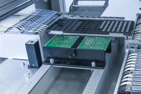
2. Component Placement
After pasting, the PCB is conveyed to a pick-and-place machine that automatically picks up and places SMT components onto their pads. Components are supplied on tape-and-reel, matrix trays, or tubes.
The machine uses a vacuum nozzle to pick up each component and a high-resolution camera to align it properly before placing it into the solder paste on the PCB. Placement force is carefully controlled. The tacky solder paste holds the components in place.
Component placement by machine is fast and precise. Fine-pitch and oddly shaped components like BGAs and QFNs can be placed accurately.
3. Reflow Soldering
Next, the populated PCB is sent through a reflow oven. The oven has multiple temperature zones that the board passes through, following a specific time/temperature profile.
The reflow profile is tailored to the solder paste formulation and PCB/component characteristics. It generally has four stages:
| Stage | Description |
|---|---|
| Preheat | PCB is slowly heated to 120-150°C. Flux becomes active, cleaning oxidation. |
| Soak | Temperature held steady at 150-180°C for 60-120 seconds. Flux activation is completed and solder paste viscosity decreases. |
| Reflow | PCB quickly heated to 20-40°C above solder melting point. In liquid state for 30-90 seconds. |
| Cooling | PCB cooled, allowing solder to solidify. Proper cooling prevents excessive intermetallic formation and thermal shock. |
The peak reflow temperature and time above liquidus are key profile parameters. They must be high/long enough to allow complete melting and wetting, but not so high/long as to cause component or PCB damage.
Convection reflow ovens are most common, using forced hot air to heat the board. The ovens have top and bottom heating zones with independent PID control to maintain the desired profile. Nitrogen gas may be used to reduce oxidation.
4. Inspection and Testing
After reflow, the PCBs are inspected, either manually or using automated optical inspection (AOI) systems. AOI uses high-resolution cameras and computer vision algorithms to check solder joints and component placement against reference images.
Electrical testing is also performed to verify proper connections and circuit function. In-circuit test (ICT) fixtures make contact with test points on the board to measure continuity and component values. Functional testing applies power and test stimuli to the board I/Os to check higher-level operation.

Solder Paste
The solder paste used is a key consumable in reflow soldering. It consists of solder powder mixed with a blend of liquid flux. The flux removes metal oxides, promotes wetting, and protects against reoxidation.
Solder pastes are formulated to meet specific rheological properties:
– Viscosity suitable for printing
– Tackiness to hold components in place
– Slump resistance to maintain printed deposit geometry
The most common solder alloys for electronics assembly are tin-lead (Sn-Pb) and lead-free tin-silver-copper (SAC). Alloy selection involves tradeoffs in processing temperatures, wetting behavior, mechanical strength, and cost.
| Alloy | Composition | Melting Temp. | Comments |
|---|---|---|---|
| Sn63-Pb37 | 63% tin, 37% lead | 183°C | Eutectic, common leaded alloy |
| SAC305 | 96.5% tin, 3% silver, 0.5% copper | 217°C | Common lead-free, general purpose |
| SAC105 | 98.5% tin, 1% silver, 0.5% copper | 227°C | Lower silver content, more economical |
The size and shape of the solder powder particles also impact paste printing and melting behavior. Spherical powders in the Type 3 size range (25-45 µm) are frequently used.
Solder paste is sensitive to storage conditions and age. Refrigerated storage extends shelf life. Viscosity and solderability must be monitored over time to ensure consistent printing and reflow results.

PCB Design Considerations for Reflow
Certain PCB design choices can make an assembly more manufacturable for reflow soldering:
Pad and Footprint Design
The component pads should be properly sized and spaced to allow sufficient solder paste printed volume and fillets. The pad layout and solder mask aperture design affect paste release from the stencil.
Thermal Design
The PCB should promote even heating and cooling during reflow. Large copper areas can act as heat sinks and cause cold solder joints. Heavy copper planes may require thermal reliefs around through-holes.
Component Selection
Components should be rated for the expected peak reflow temperatures. Some components are not suitable for reflow soldering, such as large electrolytic capacitors or connectors with low plastics.
Panelization
Splitting a large PCB design into a panel of smaller boards can aid in placement and reflow. V-scored panelization with breakaway tabs is preferred for allowing the panel to expand and contract freely during heating and cooling.

RAYPCB’s Reflow Soldering Capabilities
At RAYPCB, we specialize in Turnkey PCB assembly services using state-of-the-art reflow soldering equipment. Our capabilities include:
- High-mix, low-to-medium volume production
- Prototype and quick-turn assembly
- RoHS-Compliant lead-free soldering
- Fine pitch and BGA component placement
- Automated optical inspection (AOI)
- In-circuit and functional testing
We maintain a variety of solder paste printing equipment to handle boards from small to large format. Our automated pick-and-place machines are capable of placing a wide range of SMT components, down to 0201 sizes and fine-pitch BGAs.
Our reflow ovens are optimized for lead-free Solder profiles. The ovens use an inert nitrogen atmosphere to minimize oxidation and produce high-quality solder joints. We carefully monitor paste conditions and reflow profiles to ensure consistent results.
For more information on our PCB assembly capabilities and to get started on your next project, please contact us at RAYPCB, we are ready to apply our expertise to your OEM products.
Frequently Asked Questions (FAQ)
1. What is the difference between reflow and wave soldering?
Reflow soldering is used for surface mount components, where the entire board is heated to melt pre-applied solder paste. Wave soldering is used for through-hole components, where the board is passed over a molten solder wave to coat the component leads.
2. Can reflow soldering be used for through-hole components?
In general, no. Through-hole components are not designed to withstand the high temperatures of reflow soldering. The component leads also need to be accessible for solder wave contact. However, some through-hole components like connectors can be reflow soldered using special paste-in-hole techniques.
3. What is the shelf life of solder paste?
Solder paste shelf life depends on the specific formulation, but is typically around 6 months when refrigerated. The paste can still be used beyond this time if it passes viscosity and wetting tests, but print and reflow performance may degrade.
4. Can a PCB be reflowed multiple times?
Yes, a PCB can go through multiple reflow cycles, such as for double-sided assembly or rework. However, each additional heating cycle can degrade the solder joint quality and component reliability. The number of reflow cycles should be minimized and the reflow profiles carefully controlled to avoid damage.
5. What causes tombstoning of components during reflow?
Tombstoning is where a small two-terminal chip component stands up on end due to uneven solder melting or wetting on its pads. It can be caused by uneven solder paste printing, component misalignment, or pad designs with unequal heat absorption. Proper stencil design, print process control, and PCB layout techniques can minimize tombstoning occurrences.
No responses yet