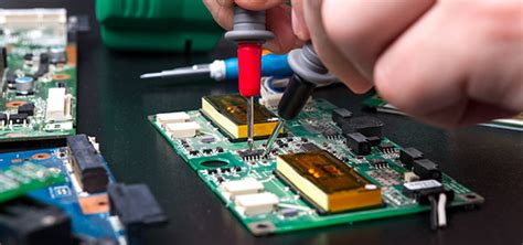
What is PCB Repair?
PCB repair refers to the process of fixing or restoring a printed circuit board (PCB) that has been damaged, either through normal wear and tear, accidental damage, or manufacturing defects. PCBs are the backbone of modern electronics, found in everything from smartphones and laptops to industrial equipment and medical devices. When a PCB fails, it can render the entire device unusable, making PCB repair an essential skill for anyone working with electronics.
PCB repair can involve a wide range of techniques, depending on the nature of the damage and the complexity of the board. Some common PCB repair methods include:
- Soldering: Replacing damaged components, traces, or pads using a soldering iron and solder.
- Jumper wires: Using thin wires to bridge damaged traces or connect components.
- Epoxy: Using conductive epoxy to fill in damaged areas or secure components.
- Trace repair: Using specialized tape or conductive ink to repair damaged traces.
- Pad repair: Replacing damaged or lifted pads using a variety of techniques.
In this article, we’ll focus specifically on PCB pad repair using Circuit Board Repair kit tape and other methods.
What is a PCB Pad?
A PCB pad is a small, usually circular or rectangular, area of exposed metal on a PCB that is used to solder components to the board. Pads are typically made of copper and are plated with a thin layer of solder to make soldering easier. Pads are connected to traces, which are thin lines of copper that carry electrical signals between components on the board.
Pads can be damaged in a number of ways, including:
- Lifting: The pad separates from the board, often due to heat or mechanical stress.
- Corrosion: The pad becomes oxidized or corroded, making soldering difficult or impossible.
- Damage: The pad is physically damaged, such as being scratched, gouged, or partially removed.
When a pad is damaged, it can be difficult or impossible to solder a component to the board, which can render the entire PCB unusable. Pad repair is therefore an essential skill for anyone working with PCBs.

PCB Pad Repair Methods
There are several methods for repairing damaged PCB pads, depending on the nature and extent of the damage. Here are some of the most common PCB pad repair methods:
1. Circuit Board Repair Kit Tape
One of the easiest and most effective ways to repair a damaged PCB pad is to use circuit board repair kit tape. This tape is a specialized adhesive tape that is designed specifically for PCB repair. It typically consists of a thin, flexible base material, such as polyimide or fiberglass, coated with a conductive adhesive.
To use circuit board repair kit tape, simply cut a small piece of tape to the appropriate size and shape, then apply it over the damaged pad. The conductive adhesive will create an electrical connection between the component and the trace, allowing the circuit to function normally.
Circuit board repair kit tape is available in a variety of sizes and shapes, including dots, squares, and custom shapes. It is also available in different thicknesses and materials to suit different applications.
Advantages of circuit board repair kit tape include:
- Easy to use: Simply cut and apply the tape over the damaged pad.
- Versatile: Can be used to repair a wide range of pad sizes and shapes.
- Durable: The tape is designed to withstand high temperatures and mechanical stress.
- Conductive: The adhesive creates an electrical connection between the component and the trace.
Disadvantages of circuit board repair kit tape include:
- Limited strength: The tape may not be strong enough to hold heavy components or withstand high levels of mechanical stress.
- Adhesive residue: The adhesive may leave a residue on the board, which can be difficult to clean.
- Cost: Circuit board repair kit tape can be relatively expensive compared to other pad repair methods.
2. Epoxy
Another common method for repairing damaged PCB pads is to use epoxy. Epoxy is a two-part adhesive that consists of a resin and a hardener. When mixed together, the epoxy cures to form a strong, durable bond.
To use epoxy for PCB pad repair, mix the resin and hardener according to the manufacturer’s instructions, then apply a small amount of the mixture to the damaged pad using a toothpick or other applicator. Place the component onto the pad and hold it in place until the epoxy cures, which typically takes several hours.
Advantages of using epoxy for PCB pad repair include:
- Strong bond: Epoxy forms a strong, durable bond that can withstand high levels of mechanical stress.
- Versatile: Epoxy can be used to repair a wide range of pad sizes and shapes.
- Inexpensive: Epoxy is relatively inexpensive compared to other pad repair methods.
Disadvantages of using epoxy for PCB pad repair include:
- Messy: Epoxy can be messy to work with and can be difficult to clean up if it gets on other parts of the board.
- Slow curing: Epoxy typically takes several hours to cure fully, which can slow down the repair process.
- Non-conductive: Standard epoxy is not conductive, so it cannot be used to create an electrical connection between the component and the trace. Conductive epoxy is available, but it is more expensive and can be more difficult to work with.
3. Jumper Wires
If a PCB pad is completely destroyed or missing, it may not be possible to repair it using tape or epoxy. In this case, one option is to use a jumper wire to connect the component directly to the trace.
To use a jumper wire for PCB pad repair, first, locate the trace that the pad was connected to. Then, solder one end of the jumper wire to the component lead and the other end to the trace. Be sure to use a thin, flexible wire and keep the connection as short as possible to minimize the risk of damage or interference.
Advantages of using jumper wires for PCB pad repair include:
- Effective: Jumper wires can be used to repair pads that are completely destroyed or missing.
- Inexpensive: Jumper wires are relatively inexpensive and readily available.
Disadvantages of using jumper wires for PCB pad repair include:
- Time-consuming: Soldering jumper wires can be time-consuming, especially if multiple pads need to be repaired.
- Fragile: Jumper wires are thin and fragile and can be easily damaged or broken if not handled carefully.
- Interference: Jumper wires can create interference or crosstalk if not routed carefully, which can affect the performance of the circuit.
4. Pad Replacement
In some cases, the best option for PCB pad repair may be to replace the damaged pad entirely. This involves removing the damaged pad and replacing it with a new one, either by soldering a new pad in place or by using a specialized pad repair kit.
To replace a damaged PCB pad, first, remove any remaining debris or solder from the area around the pad. Then, use a sharp knife or other tool to carefully cut away the damaged pad, being careful not to damage the surrounding traces or components.
Next, clean the area thoroughly with isopropyl alcohol or another suitable solvent to remove any remaining adhesive or debris. If using a pad repair kit, follow the manufacturer’s instructions for applying the new pad. If soldering a new pad in place, apply a small amount of solder paste to the area and place the new pad onto the board. Heat the pad with a soldering iron until the solder melts and the pad is securely attached to the board.
Advantages of pad replacement include:
- Durability: A properly replaced pad can be as strong and durable as the original pad.
- Aesthetics: Replacing a damaged pad can improve the appearance of the board and make it look like new.
Disadvantages of pad replacement include:
- Skill required: Replacing a pad requires a high level of skill and precision, and may not be suitable for beginners or those without access to specialized tools and equipment.
- Time-consuming: Replacing a pad can be a time-consuming process, especially if multiple pads need to be replaced.
- Cost: Pad repair kits and replacement pads can be relatively expensive compared to other repair methods.

Tips for Successful PCB Pad Repair
Regardless of which method you choose for PCB pad repair, there are several tips and best practices that can help ensure a successful repair:
-
Work in a clean, well-lit environment: PCB repair requires precision and attention to detail, so it’s important to work in a clean, well-lit area where you can see what you’re doing.
-
Use the right tools: Having the right tools and equipment can make PCB repair much easier and more effective. Invest in high-quality Soldering Irons, solder, flux, and other tools as needed.
-
Practice on scrap boards: Before attempting to repair a valuable PCB, practice your skills on scrap boards or practice kits to build confidence and technique.
-
Take your time: PCB repair is not a race, so take your time and work carefully to avoid mistakes or further damage to the board.
-
Use magnification: Many PCB repairs involve working with tiny components and traces, so using magnification can be helpful to see what you’re doing more clearly.
-
Clean the board thoroughly: Before attempting any repair, be sure to clean the board thoroughly with isopropyl alcohol or another suitable solvent to remove any dirt, grease, or other contaminants that could interfere with the repair.
-
Test the repair: After completing the repair, be sure to test the board thoroughly to ensure that it is functioning correctly and that there are no short circuits or other issues.

FAQs
1. Can I use regular adhesive tape for PCB pad repair?
No, regular adhesive tape is not suitable for PCB pad repair as it is not conductive and may not withstand the high temperatures and mechanical stresses involved in PCB Assembly and use. It’s important to use specialized circuit board repair kit tape or other conductive adhesives designed specifically for PCB repair.
2. How long does epoxy take to cure for PCB pad repair?
The curing time for epoxy can vary depending on the specific product and environmental conditions, but most epoxies used for PCB repair take several hours to cure fully. Some fast-curing epoxies may cure in as little as 5-10 minutes, while others may take up to 24 hours or more. Be sure to follow the manufacturer’s instructions carefully and allow adequate time for the epoxy to cure before handling or using the repaired board.
3. Can I use jumper wires to repair multiple damaged pads on the same board?
Yes, jumper wires can be used to repair multiple damaged pads on the same board, but it’s important to route the wires carefully to avoid interference or short circuits. If possible, use different colors of wire for each repair to make it easier to keep track of which wire goes where. Also, be sure to use thin, flexible wire and keep the connections as short as possible to minimize the risk of damage or interference.
4. How do I know which pad repair method to use?
The best pad repair method to use will depend on the nature and extent of the damage, as well as your skill level and available tools and materials. In general, circuit board repair kit tape is a good choice for minor damage or lifted pads, while epoxy or jumper wires may be better for more extensive damage. Pad replacement is typically only necessary if the pad is completely destroyed or missing. If in doubt, it’s always best to consult with a more experienced technician or refer to the manufacturer’s repair guide for guidance.
5. Can I reuse a PCB pad that has been repaired?
In most cases, a properly repaired PCB pad can be reused just like a new pad. However, the long-term durability and reliability of the repair will depend on the quality of the repair and the materials used. If the repair is not done properly, or if low-quality materials are used, the repaired pad may be more prone to failure or damage over time. To ensure the best possible results, always use high-quality materials and follow best practices for PCB repair, and test the repaired board thoroughly before putting it back into service.
Conclusion
PCB pad repair is an essential skill for anyone working with electronics, as damaged or missing pads can render an entire PCB unusable. While there are several methods for repairing damaged pads, including circuit board repair kit tape, epoxy, jumper wires, and pad replacement, the best method to use will depend on the nature and extent of the damage, as well as your skill level and available tools and materials.
By following best practices for PCB repair, including working in a clean environment, using the right tools, practicing on scrap boards, taking your time, using magnification, cleaning the board thoroughly, and testing the repair, you can increase your chances of success and ensure that your repaired board will function correctly and reliably over the long term.
Whether you’re a hobbyist or a professional technician, investing in high-quality PCB repair tools and materials and taking the time to develop your skills can pay off in the long run by saving you time, money, and frustration when dealing with damaged or malfunctioning PCBs.
No responses yet