Enjoy the best RF Design & Manufacturing combined together
18 Years RF PCB Manufacturing Experience
1000+ Clients Served
10000+ Projects Succeeded
100% satisfy clients in our work
High Quality
Solving RF technology challenges for a sustainable world
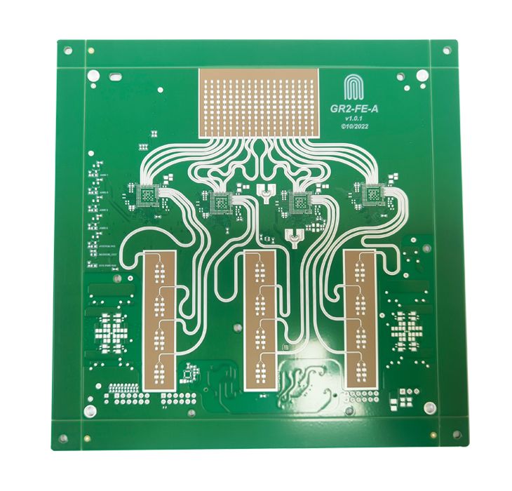
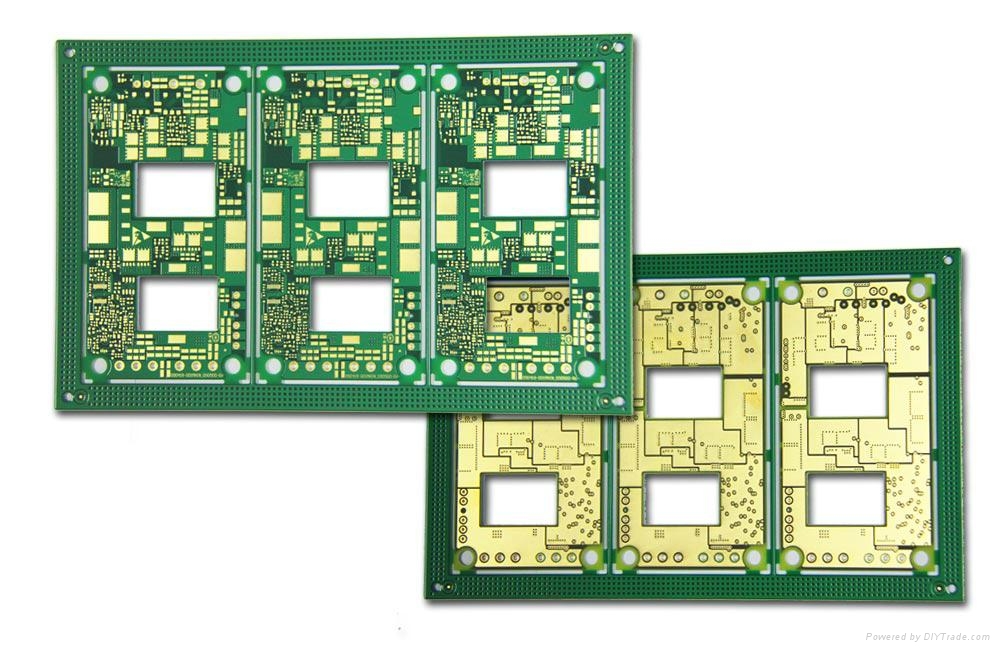
The Leading Website for the RF & Microwave Industry, The RF PCB differs from a low frequency or line frequency PCB design, as the high frequency imparts difficulties when following the standard guidelines
RF mANUFACTURING CAPABILITY
| Features | Capabilities |
|---|---|
| Layer Count | 2-44 layers |
| Drill aspect ratio | 15:1 |
| Maximum Panel Size | 24″ x 30″ |
| Vias | Blind / Buried Vias. & Micro Vias Via In Pad with Fill Options (Conductive, Non-Conductive, Copper Plug) |
| Characteristic impedance of a transmission line | Controlled impedance |
| Minimum track and gaps | 0.75mm / 0.075 mm |
| Metal Core thickness | 58mm * 1010mm |
| Surface finish | HASL (Lead-free), OSP, ENIg, immersion tin, immersion silver. |