What is PCB Testing?
PCB testing is a comprehensive process that involves subjecting a printed circuit board to various electrical, mechanical, and environmental tests to ensure that it meets the required specifications and standards. The primary goal of PCB testing is to identify and rectify any defects or issues before the board is assembled into a final product, thus minimizing the risk of product failure or malfunction.
Why is PCB Testing Important?
PCB testing is crucial for several reasons:
- Quality assurance: Testing ensures that the PCB meets the required quality standards and functions as intended.
- Cost reduction: Identifying and fixing defects early in the manufacturing process helps reduce the cost of rework and scrap.
- Reliability: Thorough testing ensures that the PCB can withstand the intended operating conditions and has a longer lifespan.
- Safety: PCB testing helps prevent potential safety hazards, such as short circuits or overheating, which could lead to fire or other dangers.
- Compliance: Testing ensures that the PCB complies with industry standards and regulations, such as RoHS (Restriction of Hazardous Substances) and UL (Underwriters Laboratories).

Types of PCB Testing
There are several types of PCB tests, each designed to evaluate different aspects of the board’s performance and quality. Some of the most common types of PCB testing include:
1. Visual Inspection
Visual inspection is the first step in the PCB testing process. It involves examining the board for any visible defects, such as scratches, cracks, or discoloration. This inspection can be performed manually or using automated optical inspection (AOI) equipment.
| Inspection Type | Description |
|---|---|
| Manual Inspection | A skilled technician visually inspects the PCB for defects using magnification tools. |
| Automated Optical Inspection (AOI) | A machine with high-resolution cameras and advanced image processing software inspects the PCB for defects. |
2. Automated Optical Inspection (AOI)
AOI is a more advanced form of visual inspection that uses high-resolution cameras and sophisticated software to detect surface-level defects on the PCB. This method is faster and more accurate than manual inspection, making it suitable for high-volume production.
| AOI Equipment | Description |
|---|---|
| 2D AOI | Inspects the PCB from a top-down view using a single camera. Suitable for detecting defects on the surface of the board. |
| 3D AOI | Uses multiple cameras or laser scanners to create a 3D model of the PCB, allowing for the detection of defects in component placement and solder joints. |
3. In-Circuit Testing (ICT)
In-circuit testing is a method of testing individual components on the PCB to ensure that they are functioning correctly and are properly connected. This test is performed using a bed-of-nails fixture, which makes contact with specific points on the board to measure resistance, capacitance, and other electrical properties.
| ICT Fixture Type | Description |
|---|---|
| Dedicated Fixture | A custom-built fixture designed for a specific PCB. Offers the highest test coverage but is more expensive and time-consuming to develop. |
| Universal Fixture | A general-purpose fixture that can be adapted to test different PCBs. Less expensive and faster to set up but may have lower test coverage. |
4. Flying Probe Testing
Flying probe testing is an alternative to ICT that uses movable probes instead of a fixed bed-of-nails fixture. This method is more flexible and can be used to test a wider variety of PCBs, but it is slower than ICT and may not provide the same level of test coverage.
| Flying Probe Tester | Description |
|---|---|
| Single-sided Tester | Uses probes on one side of the PCB. Suitable for testing simpler boards with components on only one side. |
| Double-sided Tester | Uses probes on both sides of the PCB. Can test more complex boards with components on both sides. |
5. Functional Testing
Functional testing involves testing the PCB as a complete system to ensure that it performs its intended function. This test is typically performed after the board has been fully assembled and may involve subjecting the board to various stimuli, such as temperature changes or vibrations, to simulate real-world operating conditions.
| Functional Test Type | Description |
|---|---|
| Boundary Scan Testing | Uses built-in test circuitry (JTAG) to test the interconnections between components on the PCB. |
| JTAG Testing | A type of boundary scan testing that uses the JTAG (Joint Test Action Group) standard for testing and debugging PCBs. |
6. Burn-In Testing
Burn-in testing involves subjecting the PCB to elevated temperatures and voltages for an extended period to identify any components that may fail prematurely. This test helps to eliminate early failures and improve the overall reliability of the board.
| Burn-In Test Parameter | Description |
|---|---|
| Temperature | The temperature at which the PCB is tested, typically higher than the normal operating temperature. |
| Duration | The length of time the PCB is subjected to the elevated temperature, usually several hours or days. |
| Voltage | The voltage applied to the PCB during the test, which may be higher than the normal operating voltage. |
7. Environmental Testing
Environmental testing involves subjecting the PCB to various environmental conditions, such as temperature extremes, humidity, and vibration, to ensure that it can operate reliably in its intended environment. This type of testing is particularly important for PCBs that will be used in harsh or demanding applications, such as automotive or aerospace electronics.
| Environmental Test Type | Description |
|---|---|
| Temperature Cycling | Exposes the PCB to alternating high and low temperatures to simulate thermal stress. |
| Humidity Testing | Subjects the PCB to high humidity levels to evaluate its resistance to moisture. |
| Vibration Testing | Tests the PCB’s ability to withstand mechanical vibrations and shocks. |
| Altitude Testing | Simulates the effects of high altitude on the PCB, including reduced air pressure and cooling efficiency. |

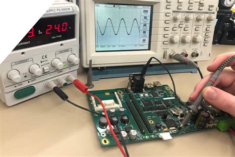
PCB Testing Equipment
To perform the various types of PCB tests, manufacturers use a range of specialized equipment. Some of the most common PCB testing equipment includes:
- Multimeters: Used to measure voltage, current, and resistance on the PCB.
- Oscilloscopes: Used to visualize and analyze electrical signals on the PCB.
- Logic Analyzers: Used to capture and analyze digital signals on the PCB.
- Spectrum Analyzers: Used to measure and analyze the frequency response of the PCB.
- LCR Meters: Used to measure inductance, capacitance, and resistance of components on the PCB.
- Thermal Cameras: Used to identify hot spots and thermal issues on the PCB.
| Equipment | Description |
|---|---|
| Multimeter | A basic tool used to measure voltage, current, and resistance on the PCB. |
| Oscilloscope | A more advanced tool used to visualize and analyze electrical signals on the PCB. |
| Logic Analyzer | A specialized tool used to capture and analyze digital signals on the PCB. |
| Spectrum Analyzer | A tool used to measure and analyze the frequency response of the PCB. |
| LCR Meter | A meter used to measure inductance, capacitance, and resistance of components on the PCB. |
| Thermal Camera | A camera used to identify hot spots and thermal issues on the PCB. |

PCB Testing Standards and Regulations
PCB testing is governed by various industry standards and regulations to ensure consistency and reliability across different manufacturers and applications. Some of the most important PCB testing standards include:
- IPC-A-610: Acceptability of Electronic Assemblies
- IPC-6012: Qualification and Performance Specification for Rigid Printed Boards
- IPC-A-600: Acceptability of Printed Boards
- J-STD-001: Requirements for Soldered Electrical and Electronic Assemblies
- IPC-TM-650: Test Methods Manual
| Standard | Description |
|---|---|
| IPC-A-610 | Defines the acceptability criteria for electronic assemblies, including PCBs. |
| IPC-6012 | Specifies the requirements for the qualification and performance of rigid printed boards. |
| IPC-A-600 | Establishes the acceptability criteria for printed boards before assembly. |
| J-STD-001 | Outlines the requirements for soldered electrical and electronic assemblies. |
| IPC-TM-650 | A comprehensive manual containing various test methods for PCBs and electronic assemblies. |
FAQ
1. How long does PCB testing take?
The duration of PCB testing depends on the complexity of the board, the types of tests performed, and the number of boards being tested. Simple boards may take a few minutes to test, while more complex boards can take several hours or even days. Factors that can impact testing time include the number of components on the board, the size of the board, and the specific testing requirements.
2. Can PCB testing be performed in-house?
Yes, some PCB testing can be performed in-house if the manufacturer has the necessary equipment and expertise. However, more advanced testing, such as environmental testing or high-volume production testing, may require specialized facilities and equipment that are more commonly found at dedicated testing service providers.
3. How much does PCB testing cost?
The cost of PCB testing varies depending on the type and extent of testing required, as well as the volume of boards being tested. Simple tests, such as visual inspection or basic electrical testing, may cost a few cents per board, while more advanced tests, such as burn-in or environmental testing, can cost several dollars per board. Manufacturers should work with their testing service provider to determine the most cost-effective testing strategy for their specific needs.
4. What happens if a PCB fails a test?
If a PCB fails a test, the manufacturer must investigate the cause of the failure and take appropriate corrective action. This may involve modifying the PCB design, adjusting the manufacturing process, or reworking the affected boards. In some cases, the entire batch of boards may need to be scrapped if the issue cannot be resolved. Thorough testing and early detection of issues can help minimize the cost and impact of PCB failures.
5. Are there any industry certifications for PCB testing?
Yes, there are several industry certifications that demonstrate a manufacturer’s commitment to quality and adherence to industry standards. Some of the most common certifications include:
- ISO 9001: Quality Management Systems
- IPC-A-610: Acceptability of Electronic Assemblies
- J-STD-001: Requirements for Soldered Electrical and Electronic Assemblies
- UL (Underwriters Laboratories) Certification
Manufacturers that hold these certifications have demonstrated their ability to consistently produce high-quality PCBs that meet the relevant industry standards.
Conclusion
PCB testing is a critical aspect of the electronics manufacturing process, ensuring that printed circuit boards meet the required quality, reliability, and safety standards. By understanding the various types of tests, equipment, and standards involved in PCB testing, manufacturers can develop effective testing strategies that minimize defects, reduce costs, and improve overall product quality. As electronic devices continue to become more complex and sophisticated, the importance of rigorous PCB testing will only continue to grow, making it an essential consideration for any electronics manufacturer.
No responses yet