Introduction to PCB Assembly
Printed Circuit Board (PCB) assembly is the process of soldering or mounting electronic components onto a PCB. This process is crucial in the manufacturing of electronic devices, as it determines the functionality, reliability, and quality of the final product. In this comprehensive article, we will delve into the various aspects of PCB assembly, including the types of PCB assembly, the process involved, and the best practices for ensuring high-quality results.
Types of PCB Assembly
There are three main types of PCB assembly:
-
Through-Hole Assembly (THA): This is the traditional method of PCB assembly, where component leads are inserted through drilled holes in the PCB and soldered onto the opposite side.
-
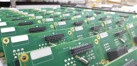
Surface Mount Assembly (SMA): In this method, components are placed directly onto the surface of the PCB and soldered using a reflow oven or wave soldering machine.
-
Mixed Technology Assembly: This method combines both THA and SMA techniques to accommodate different component types on the same PCB.
| Assembly Type | Advantages | Disadvantages |
|---|---|---|
| Through-Hole Assembly | – Strong mechanical bonds – Easy to replace components – Suitable for high-power applications |
– Larger component size – Higher manufacturing costs – Limited PCB real estate |
| Surface Mount Assembly | – Smaller component size – Higher component density – Faster assembly process – Lower manufacturing costs |
– Requires specialized equipment – More difficult to replace components – Not suitable for high-power applications |
| Mixed Technology Assembly | – Combines advantages of THA and SMA – Accommodates diverse component types |
– More complex assembly process – Higher manufacturing costs |
The PCB Assembly Process
The PCB assembly process consists of several steps, each of which is critical to ensuring the quality and reliability of the final product.
Step 1: Solder Paste Application
The first step in the PCB assembly process is to apply solder paste to the PCB pads. This is typically done using a stencil and a solder paste printer. The stencil is a thin metal sheet with apertures that match the PCB pad layout, allowing the solder paste to be deposited accurately.
Step 2: Component Placement
Once the solder paste has been applied, the next step is to place the components onto the PCB. This is usually done using a pick-and-place machine, which uses vacuum nozzles to pick up components from reels or trays and place them onto the PCB with high precision.
Step 3: Reflow Soldering
After the components have been placed, the PCB is then sent through a reflow oven. The reflow oven heats the PCB and components to a specific temperature profile, causing the solder paste to melt and form a strong mechanical and electrical bond between the components and the PCB pads.
Step 4: Inspection and Testing
Once the PCB has cooled, it undergoes a series of inspections and tests to ensure that it meets the required quality standards. This may include visual inspection, automated optical inspection (AOI), X-ray inspection, and electrical testing.
Step 5: Conformal Coating and Potting (Optional)
Depending on the application and environment in which the PCB will be used, it may be necessary to apply a conformal coating or potting compound to protect the components and PCB from moisture, dust, and other environmental factors.

Best Practices for High-Quality PCB Assembly
To ensure high-quality PCB assembly, there are several best practices that should be followed:
-
Design for Manufacturing (DFM): The PCB design should be optimized for manufacturability, taking into account factors such as component placement, pad size, and spacing.
-
Use High-Quality Components: Using high-quality components from reputable suppliers can help to minimize the risk of defects and failures.
-
Implement Proper Storage and Handling: Components and PCBs should be stored and handled properly to prevent damage from electrostatic discharge (ESD), moisture, and other factors.
-
Follow Industry Standards: Adhering to industry standards such as IPC-A-610 can help to ensure consistency and quality in the PCB assembly process.
-
Conduct Thorough Testing: Comprehensive testing, including functional testing, boundary scan testing, and burn-in testing, can help to identify and eliminate defects before the final product is shipped.

Challenges in PCB Assembly
Despite the many advances in PCB assembly technology, there are still several challenges that manufacturers face:
-
Miniaturization: As electronic devices continue to shrink in size, PCB assembly becomes more challenging due to the smaller component sizes and tighter spacing requirements.
-
High-Density Interconnect (HDI): HDI PCBs, which have a higher density of interconnects and smaller via sizes, require specialized equipment and processes for assembly.
-
Lead-Free Soldering: The transition to lead-free soldering, driven by environmental regulations, has presented challenges in terms of process control and reliability.
-
Supply Chain Management: Ensuring a stable and reliable supply of components can be challenging, particularly in times of high demand or supply disruptions.

Future Trends in PCB Assembly
As technology continues to advance, there are several trends that are shaping the future of PCB assembly:
-
Automation and Robotics: The increasing use of automation and robotics in PCB assembly is helping to improve efficiency, accuracy, and consistency.
-
3D Printing: The emergence of 3D printing technology is enabling the rapid prototyping and low-volume production of PCBs and components.
-
Internet of Things (IoT): The growth of the IoT is driving demand for smaller, more complex PCBs that can be integrated into a wide range of devices and applications.
-
Advanced Materials: The development of advanced materials, such as graphene and carbon nanotubes, is opening up new possibilities for PCB design and performance.
Conclusion
PCB assembly is a critical process in the manufacturing of electronic devices, and understanding the various aspects of PCB assembly is essential for ensuring high-quality, reliable products. By following best practices, staying up-to-date with industry trends, and investing in advanced technologies and processes, manufacturers can overcome the challenges of PCB assembly and deliver innovative, high-performance electronic products to market.
Frequently Asked Questions (FAQ)
1. What is the difference between through-hole and surface mount assembly?
Through-hole assembly involves inserting component leads through drilled holes in the PCB and soldering them on the opposite side, while surface mount assembly involves placing components directly onto the surface of the PCB and soldering them using a reflow oven or wave soldering machine.
2. What is solder paste, and how is it applied to the PCB?
Solder paste is a mixture of tiny solder particles and flux that is used to form the electrical and mechanical connection between components and PCB pads. It is typically applied to the PCB using a stencil and a solder paste printer.
3. What is a pick-and-place machine, and how does it work?
A pick-and-place machine is an automated machine that is used to place components onto the PCB with high precision. It uses vacuum nozzles to pick up components from reels or trays and place them onto the PCB according to the programmed layout.
4. What is a reflow oven, and how does it work?
A reflow oven is a specialized oven that is used to melt the solder paste and form a strong bond between the components and the PCB pads. It heats the PCB and components to a specific temperature profile, causing the solder paste to melt and then cool, forming a solid joint.
5. What are some of the challenges in PCB assembly, and how can they be overcome?
Some of the challenges in PCB assembly include miniaturization, high-density interconnect, lead-free soldering, and supply chain management. These challenges can be overcome by investing in advanced technologies and processes, following best practices, and staying up-to-date with industry trends and standards.
No responses yet