Introduction to PCB Size Calculation
Printed Circuit Boards (PCBs) are essential components in modern electronic devices. They provide a platform for mounting and connecting various electronic components, such as resistors, capacitors, and integrated circuits. Calculating the size of a PCB is a crucial step in the design process, as it determines the overall dimensions of the board and affects its functionality, manufacturing cost, and compatibility with other components.
In this article, we will explore the factors that influence PCB size calculation and provide a step-by-step guide on how to determine the appropriate dimensions for your PCB design.
Factors Affecting PCB Size
Component Placement and Routing
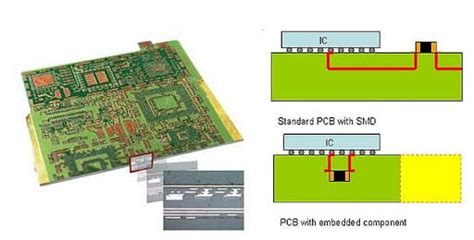
The primary factor that determines the size of a PCB is the placement and routing of electronic components. The number, type, and size of components used in the design directly impact the required board area. Additionally, the spacing between components and the width of the traces connecting them also contribute to the overall size of the PCB.
PCB Layers
PCBs can be designed with multiple layers, allowing for more complex routing and component placement. The number of layers in a PCB affects its thickness and, consequently, its size. Single-layer boards are thinner and more compact, while multi-layer boards are thicker but offer more flexibility in terms of component placement and signal routing.
| Number of Layers | Typical Thickness (mm) |
|---|---|
| 1 | 0.4 – 0.8 |
| 2 | 0.8 – 1.6 |
| 4 | 1.6 – 2.4 |
| 6 | 2.4 – 3.2 |
| 8 | 3.2 – 4.0 |
Manufacturing Constraints
PCB manufacturing processes impose certain constraints on the minimum and maximum sizes of the board. These constraints are determined by the capabilities of the manufacturing equipment and the materials used. For example, the minimum trace width and spacing, hole sizes, and Board Thickness are all subject to manufacturing limitations.
| Manufacturing Constraint | Typical Value |
|---|---|
| Minimum Trace Width | 0.1 mm |
| Minimum Trace Spacing | 0.1 mm |
| Minimum Hole Size | 0.3 mm |
| Maximum Board Thickness | 4.0 mm |

Step-by-Step Guide to Calculating PCB Size
Step 1: Determine Component Placement
Begin by identifying all the components required for your PCB design. Create a rough layout of the components on the board, considering their dimensions and the necessary spacing between them. This initial placement will give you an idea of the minimum board area required to accommodate all components.
Step 2: Consider Routing Requirements
Next, consider the routing requirements for your PCB design. Determine the number of layers needed to accommodate the desired signal routing and power distribution. Keep in mind that more layers will increase the thickness of the board, which may affect its overall size.
Step 3: Apply Manufacturing Constraints
Review the manufacturing constraints imposed by your chosen PCB fabrication process. Ensure that your design adheres to the minimum trace width, spacing, and hole sizes specified by the manufacturer. Adjust your component placement and routing as necessary to comply with these constraints.
Step 4: Calculate Board Dimensions
Based on the component placement, routing requirements, and manufacturing constraints, calculate the minimum board dimensions required to accommodate your design. Add a margin of 10-20% to the calculated dimensions to allow for any unforeseen changes or additions to the design.
| PCB Size Calculation Example | |
|---|---|
| Minimum Component Area | 50 mm x 70 mm |
| Routing Area | 20 mm x 20 mm |
| Manufacturing Margin | 10% |
| Final Board Size | (50 + 20) x 1.1 = 77 mm |
| (70 + 20) x 1.1 = 99 mm |
Step 5: Optimize and Iterate
Review your calculated board dimensions and consider opportunities for optimization. Can the component placement be more compact? Can the routing be simplified to reduce the number of layers? Iterate on your design, making adjustments to minimize the board size while maintaining functionality and manufacturability.

FAQ
1. What is the minimum size for a PCB?
The minimum size of a PCB is determined by the manufacturing constraints of the chosen fabrication process. Typically, the minimum board size is limited by the smallest trace width, spacing, and hole sizes that can be reliably manufactured. Consult with your PCB manufacturer to determine the minimum board size they can accommodate.
2. How does the number of layers affect PCB size?
The number of layers in a PCB directly affects its thickness. Each additional layer increases the overall thickness of the board, which may impact its size. However, using more layers can also allow for more compact component placement and routing, potentially reducing the required board area.
3. Can I reduce the size of my PCB by using smaller components?
Yes, using smaller components can help reduce the overall size of your PCB. Surface-mount devices (SMDs) are generally smaller than through-hole components, allowing for more compact designs. However, keep in mind that smaller components may be more challenging to work with during assembly and may have limited power handling capabilities.
4. How much margin should I add to my calculated PCB size?
It is recommended to add a margin of 10-20% to your calculated PCB dimensions. This margin accounts for any unforeseen changes or additions to the design and provides some flexibility during the manufacturing process. The exact margin required may vary depending on the complexity of your design and the manufacturing tolerances of your chosen PCB fabricator.
5. Can I use software tools to calculate PCB size?
Yes, there are various PCB design software tools available that can assist in calculating board dimensions. These tools often provide features for component placement, routing, and design rule checking, which can help optimize your PCB size. Popular PCB design software includes Altium Designer, KiCad, and Eagle.

Conclusion
Calculating the size of a PCB is a critical step in the design process, as it directly impacts the functionality, manufacturing cost, and compatibility of the final product. By considering factors such as component placement, routing requirements, and manufacturing constraints, you can determine the appropriate dimensions for your PCB design.
Remember to optimize your design through iterative refinements and always consult with your PCB manufacturer to ensure that your design meets their specific requirements. With careful planning and attention to detail, you can create compact, efficient, and manufacturable PCBs that meet the needs of your electronic projects.
No responses yet