Introduction to Innerlayer Imaging
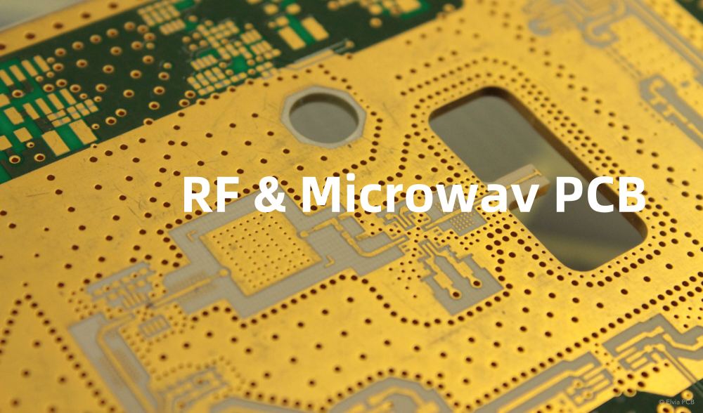
Innerlayer imaging is a critical step in the fabrication process for multilayer printed circuit boards (PCBs). It involves transferring the circuit pattern onto the copper clad laminate that will form the inner layers of the finished multilayer PCB.
The innerlayer imaging process has a significant impact on the quality, reliability, and functionality of the final PCB product. Achieving precise and defect-free innerlayer images is essential for ensuring proper connectivity between layers and preventing issues like open or short circuits.
In this article, we’ll dive deep into the topic of innerlayer imaging for multilayer PCBs. We’ll cover the different methods used, key considerations and challenges, best practices, and frequently asked questions. By the end, you’ll have a thorough understanding of this important PCB manufacturing process.
Innerlayer Imaging Methods
There are several methods used for innerlayer imaging in Multilayer PCB Fabrication. The choice of method depends on factors such as the desired feature size, throughput requirements, and available equipment. Let’s look at the most common innerlayer imaging methods:
Photolithography
Photolithography is the most widely used method for innerlayer imaging. It involves applying a light-sensitive photoresist coating onto the copper clad laminate. The photoresist is then exposed to UV light through a photomask or phototool, which contains the negative image of the desired circuit pattern.
The exposure to UV light causes a chemical change in the photoresist. For negative photoresists, the exposed areas become insoluble, while for positive photoresists, the exposed areas become soluble. After exposure, the photoresist is developed, removing the soluble areas and leaving behind the desired circuit pattern.
Photolithography allows for high-resolution imaging and is suitable for a wide range of feature sizes. However, it requires the use of expensive phototools and alignment equipment.
Direct Imaging (DI)
Direct imaging is a newer method that has gained popularity in recent years. Instead of using a photomask, DI systems use a laser or LED light source to directly expose the photoresist with the circuit pattern.
The main advantage of DI is that it eliminates the need for phototools, reducing costs and turnaround times. DI also allows for more flexibility in design changes, as the circuit pattern can be easily modified in the digital file.
However, DI systems have limitations in terms of resolution and throughput compared to photolithography. They are most suitable for prototype or low-volume production.
Laser Direct Imaging (LDI)
Laser direct imaging is a specific type of DI that uses a high-powered laser to expose the photoresist. LDI systems offer higher resolution and precision compared to LED-based DI systems.
LDI is particularly useful for imaging fine features and high-density designs. It also allows for the imaging of multiple layers in a single pass, reducing registration errors.
The main drawback of LDI is the high equipment cost and the need for specialized operators.
Key Considerations for Innerlayer Imaging
To achieve high-quality innerlayer images, several key factors must be considered:
Material Selection
The choice of laminate material and copper foil thickness can affect the innerlayer imaging process. Factors to consider include:
- Dimensional stability: The laminate should have minimal shrinkage or expansion during processing to maintain registration accuracy.
- Surface roughness: A smooth copper surface is desirable for optimal photoresist adhesion and resolution.
- Copper foil thickness: Thinner foils are more challenging to etch and may require adjustments to the imaging parameters.
Photoresist Selection
The type and thickness of the photoresist used for innerlayer imaging impact the resolution and edge quality of the circuit pattern. Key considerations include:
- Resolution: The photoresist should be capable of resolving the smallest features in the design.
- Adhesion: Good adhesion to the copper surface is necessary to prevent lifting or undercutting during development and etching.
- Thickness: Thicker photoresists provide better etch resistance but may limit resolution. Thinner photoresists offer higher resolution but may not withstand longer etch times.
Exposure and Development Parameters
Proper exposure and development of the photoresist are critical for achieving the desired circuit pattern. Factors to optimize include:
- Exposure dose: The amount of UV light energy delivered to the photoresist must be sufficient to cause the desired chemical change without overexposing.
- Exposure time: The duration of exposure should be carefully controlled to ensure consistent results.
- Development time and temperature: The development process should remove all the soluble photoresist without attacking the desired pattern. Optimal development time and temperature vary depending on the photoresist type and thickness.
Etching
After the innerlayer image is developed, the exposed copper is etched away, leaving behind the desired circuit pattern. Key considerations for etching include:
- Etch rate: The etch rate must be carefully controlled to prevent over-etching or undercutting of the Circuit Traces.
- Etch factor: The etch factor, or the ratio of vertical to horizontal etching, affects the final trace geometry and should be optimized for the desired trace width and spacing.
- Etch uniformity: Consistent etching across the entire panel is necessary to maintain the integrity of the circuit pattern.

Challenges in Innerlayer Imaging
Innerlayer imaging for multilayer PCBs presents several challenges that must be addressed to ensure high-quality results:
Registration Accuracy
In multilayer PCBs, the innerlayer images must be accurately aligned, or registered, with each other to ensure proper connectivity between layers. Factors that can affect registration accuracy include:
- Laminate shrinkage or expansion during processing
- Misalignment of the photomask or phototool
- Mechanical tolerances of the imaging equipment
To minimize registration errors, strict process controls and high-precision alignment systems are necessary.
Copper Surface Quality
The quality of the copper surface can impact the adhesion and resolution of the photoresist. Common surface defects include:
- Scratches or dents
- Oxidation or contamination
- Roughness or porosity
Proper handling, storage, and cleaning of the copper clad laminates are essential for maintaining surface quality.
Dust and Contamination
Dust and other contaminants can cause defects in the innerlayer image, such as pinholes, shorts, or opens. Sources of contamination include:
- Airborne particles in the processing environment
- Residues from cleaning or etching processes
- Debris from handling or transportation
Maintaining a clean and controlled processing environment, as well as implementing strict cleanliness protocols, can help mitigate the risk of contamination.
Best Practices for Innerlayer Imaging
To achieve the best results in innerlayer imaging for multilayer PCBs, consider the following best practices:
- Use high-quality laminates and copper foils with consistent properties and minimal defects.
- Select the appropriate photoresist and imaging method for the desired feature size and throughput.
- Optimize exposure, development, and etching parameters through systematic experimentation and process control.
- Implement strict cleanliness protocols and maintain a controlled processing environment to minimize contamination.
- Use high-precision alignment systems and registration marks to ensure accurate layer-to-layer registration.
- Conduct thorough inspections and quality checks at each stage of the innerlayer imaging process to identify and correct defects early.
- Continuously monitor and optimize the process through statistical process control (SPC) and root cause analysis of defects.
FAQ
1. What is the minimum feature size achievable with photolithography for innerlayer imaging?
The minimum feature size achievable with photolithography depends on several factors, including the wavelength of the UV light source, the type of photoresist, and the quality of the photomask. In general, modern photolithography systems can achieve feature sizes down to 25-50 microns (µm) for innerlayer imaging. However, advanced systems with optimized processes can potentially achieve even smaller feature sizes.
2. Can direct imaging be used for high-volume production of multilayer PCBs?
While direct imaging offers advantages in terms of flexibility and reduced costs for phototools, it may not be the most suitable option for high-volume production. DI systems typically have lower throughput compared to photolithography, which can be a bottleneck in high-volume manufacturing. However, advances in DI technology, such as multi-beam systems and faster data transfer rates, are improving the throughput capabilities of DI for volume production.
3. What is the purpose of copper surface roughening before innerlayer imaging?
Copper surface roughening, also known as micro-etching, is sometimes performed before innerlayer imaging to improve the adhesion of the photoresist to the copper surface. A slightly roughened surface provides better mechanical anchoring for the photoresist, reducing the risk of lifting or undercutting during development and etching. However, excessive roughening can negatively impact the resolution and uniformity of the innerlayer image.
4. How does the choice of etchant affect the innerlayer imaging process?
The choice of etchant can have a significant impact on the quality and consistency of the innerlayer image. The most common etchants used for copper etching in PCB manufacturing are acidic solutions, such as cupric chloride and ferric chloride. The etchant chemistry, concentration, and temperature affect the etch rate, etch factor, and selectivity. Proper selection and control of the etchant are necessary to achieve the desired trace geometry and to prevent over-etching or undercutting.
5. What are the advantages of using laser direct imaging (LDI) for innerlayer imaging?
Laser direct imaging offers several advantages for innerlayer imaging in multilayer PCBs:
- High resolution: LDI systems can achieve very fine feature sizes, down to 25 microns or less, making them suitable for high-density designs.
- Improved registration accuracy: LDI allows for the imaging of multiple layers in a single pass, reducing the risk of misalignment between layers.
- Reduced setup times: LDI eliminates the need for phototools, reducing the time and cost associated with phototool creation and alignment.
- Flexibility in design changes: Circuit patterns can be easily modified in the digital file, allowing for rapid design iterations without the need for new phototools.
- Improved throughput: Advanced LDI systems with multiple laser beams and high-speed data transfer can offer higher throughput compared to traditional photolithography.
However, LDI systems have higher equipment costs and require specialized operators, which should be considered when evaluating their suitability for a specific manufacturing environment.
Conclusion
Innerlayer imaging is a critical process in the fabrication of multilayer PCBs, directly impacting the quality, reliability, and functionality of the final product. By understanding the different imaging methods, key considerations, challenges, and best practices, PCB manufacturers can optimize their innerlayer imaging process to achieve high-quality results consistently.
As PCB designs continue to push the limits of complexity and density, advancements in imaging technology, such as direct imaging and laser direct imaging, offer new opportunities for improving the capabilities and efficiency of innerlayer imaging. However, the choice of imaging method must be carefully evaluated based on the specific requirements and constraints of each project.
Ultimately, a robust and well-controlled innerlayer imaging process is essential for the successful fabrication of high-quality multilayer PCBs. By continuously monitoring, optimizing, and adapting their processes, PCB manufacturers can stay at the forefront of this critical technology.
Innerlayer Imaging Methods Comparison
| Method | Resolution | Throughput | Phototool Required | Equipment Cost |
|---|---|---|---|---|
| Photolithography | High | High | Yes | Moderate to High |
| Direct Imaging | Moderate | Moderate | No | Moderate |
| Laser Direct Imaging | Very High | High | No | High |

No responses yet