Introduction to PCB Inspection
Printed Circuit Board (PCB) inspection is a crucial step in the manufacturing process to ensure the quality and reliability of electronic devices. PCB inspection involves examining the board for any defects, such as short circuits, open circuits, incorrect component placement, and soldering issues. In this article, we will discuss various methods and techniques used for PCB inspection.
Why is PCB Inspection Important?
PCB inspection is essential for several reasons:
-
Quality assurance: PCB inspection helps identify and rectify defects before the board is assembled into the final product, ensuring the overall quality of the electronic device.
-
Cost-effectiveness: Detecting and fixing issues early in the manufacturing process is more cost-effective than addressing problems after the product is assembled or shipped to customers.
-
Reliability: Thorough PCB inspection ensures that the electronic device functions as intended and reduces the risk of failures or malfunctions.
-
Compliance: PCB inspection helps manufacturers meet industry standards and regulations, such as IPC (Institute of Printed Circuits) standards.

Types of PCB Inspection
There are several types of PCB inspection techniques used in the industry:
Visual Inspection
Visual inspection is the most basic form of PCB inspection, where the board is examined with the naked eye or using magnifying lenses. This method is suitable for identifying obvious defects, such as incorrect component placement, solder bridges, or damaged components.
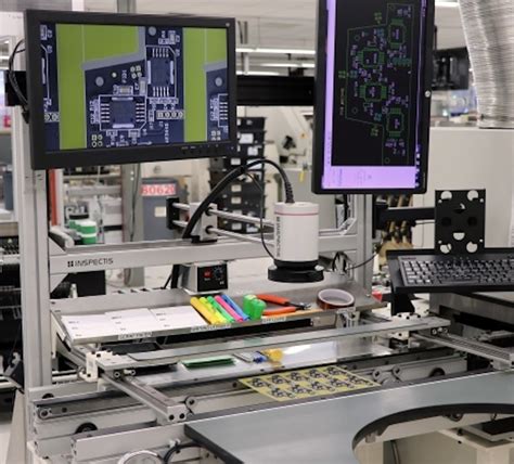
Automated Optical Inspection (AOI)
AOI uses high-resolution cameras and image processing software to inspect PCBs automatically. The system compares the captured images with a reference image of a defect-free board to identify any anomalies. AOI is faster and more accurate than manual visual inspection and can detect a wide range of defects, including:
- Solder joint defects (e.g., insufficient solder, solder bridges)
- Component placement errors
- Missing or incorrect components
- Polarity issues
- Trace defects (e.g., open circuits, short circuits)
X-Ray Inspection
X-ray inspection is used to examine hidden features or defects that are not visible on the surface of the PCB. This method is particularly useful for inspecting ball grid array (BGA) packages, flip chips, and other components with hidden solder joints. X-ray inspection systems use either 2D or 3D imaging techniques to detect:
- Solder joint defects (e.g., voids, insufficient solder)
- Component placement errors
- Internal component defects
- Counterfeit components
In-Circuit Testing (ICT)
ICT is a functional testing method that verifies the electrical connectivity and performance of individual components on the PCB. The board is placed on a bed-of-nails fixture, which makes contact with specific test points on the board. The system then applies electrical signals and measures the response to detect:
- Short circuits
- Open circuits
- Incorrect component values
- Faulty components
Functional Testing
Functional testing involves testing the PCB as a complete system to ensure that it performs as intended. This method typically requires the board to be fully assembled and powered on. Functional testing can be performed manually or using automated test equipment (ATE) to verify:
- Power supply functionality
- Signal integrity
- Communication interfaces
- Overall system performance

PCB Inspection Standards
The electronics industry has established several standards for PCB inspection to ensure consistency and reliability. The most widely recognized standards are those developed by the IPC.
| Standard | Description |
|---|---|
| IPC-A-610 | Acceptability of Electronic Assemblies |
| IPC-A-600 | Acceptability of Printed Boards |
| IPC-6012 | Qualification and Performance Specification for Rigid Printed Boards |
| IPC-6013 | Qualification and Performance Specification for Flexible Printed Boards |
| IPC-6018 | Microwave End Product Board Inspection and Test |
These standards provide guidelines for various aspects of PCB inspection, including:
- Workmanship requirements
- Acceptance criteria for defects
- Inspection methods and equipment
- Documentation and reporting

Best Practices for PCB Inspection
To ensure effective and efficient PCB inspection, consider the following best practices:
-
Develop a comprehensive inspection plan that covers all stages of the manufacturing process, from Bare Board inspection to final functional testing.
-
Train inspectors to identify and classify defects according to industry standards and company guidelines.
-
Use appropriate inspection equipment and techniques for each type of PCB and component package.
-
Establish clear acceptance criteria for defects based on industry standards and customer requirements.
-
Maintain accurate documentation of inspection results, including defect types, locations, and corrective actions taken.
-
Continuously monitor and analyze inspection data to identify trends and opportunities for process improvement.
-
Regularly calibrate and maintain inspection equipment to ensure accurate and consistent results.
-
Foster a culture of quality and continuous improvement throughout the organization, encouraging collaboration between design, manufacturing, and quality teams.
Frequently Asked Questions (FAQ)
- What is the difference between AOI and visual inspection?
-
AOI uses automated cameras and image processing software to inspect PCBs, while visual inspection relies on human vision and judgment. AOI is faster, more consistent, and can detect a wider range of defects compared to visual inspection.
-
Can X-ray inspection detect counterfeit components?
-
Yes, X-ray inspection can help identify counterfeit components by revealing internal differences in construction or material composition compared to genuine components.
-
How often should PCB inspection equipment be calibrated?
-
Calibration frequency depends on the specific equipment and the manufacturer’s recommendations. In general, inspection equipment should be calibrated at least annually or whenever there are significant changes in the manufacturing process or environment.
-
What is the role of IPC Standards in PCB inspection?
-
IPC standards provide guidelines and acceptance criteria for various aspects of PCB inspection, helping to ensure consistency and reliability across the industry. Adhering to IPC standards can help manufacturers meet customer requirements and regulatory compliance.
-
How can inspection data be used for process improvement?
- Inspection data can be analyzed to identify patterns or trends in defect types, locations, or frequencies. This information can be used to identify root causes of problems and implement corrective actions to improve the manufacturing process, such as adjusting equipment settings, updating work instructions, or providing additional training to operators.
Conclusion
PCB inspection is a critical process in ensuring the quality, reliability, and functionality of electronic devices. By employing a combination of visual, automated, and functional testing methods, manufacturers can detect and rectify defects early in the production process, reducing costs and improving customer satisfaction. Adhering to industry standards and best practices for PCB inspection can help organizations maintain a competitive edge in the ever-evolving electronics industry.
No responses yet