What is PCB Bow and Twist?
PCB bow and twist are common issues that can arise during the manufacturing process of printed circuit boards (PCBs). These defects refer to the warping or distortion of the board, which can lead to various problems, such as component misalignment, soldering difficulties, and reduced reliability.
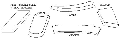
Bow
PCB bow is the curvature of the board along its length or width. It is measured as the maximum deviation from a flat surface, typically expressed in millimeters or mils (thousandths of an inch). Bow can occur in either a concave or convex direction, depending on the specific manufacturing conditions and material properties.
Twist
PCB twist, on the other hand, is the rotation of the board along its diagonal axis. It is measured as the maximum deviation from a flat surface at the corners of the board, also expressed in millimeters or mils. Twist can occur in a clockwise or counterclockwise direction and is often caused by uneven stress distribution during the manufacturing process.
Causes of PCB Bow and Twist
Several factors can contribute to the development of bow and twist in PCBs:
Material Properties
The choice of substrate material and its inherent properties play a significant role in the occurrence of bow and twist. Different materials have varying coefficients of thermal expansion (CTE), which determine how much they expand or contract when subjected to temperature changes. Mismatches in CTE between the substrate, copper layers, and other materials used in the PCB can lead to warping.
Manufacturing Process
The manufacturing process itself can introduce stresses that cause bow and twist. For example, during the lamination process, where layers of the PCB are bonded together under high pressure and temperature, uneven pressure distribution or temperature gradients can result in warping. Similarly, during the cooling phase, if the board is not allowed to cool down uniformly, it can develop bow or twist.
Copper Distribution
The distribution of copper on the PCB can also influence the occurrence of bow and twist. If the copper is not evenly distributed across the layers, it can create an imbalance in the mechanical stresses, leading to warping. This is particularly relevant for boards with high copper coverage or those with large copper planes.
Environmental Factors
Environmental factors, such as humidity and temperature variations, can also contribute to PCB bow and twist. If the board is exposed to extreme or fluctuating environmental conditions, it can absorb moisture or experience thermal stresses, resulting in warping.

Effects of PCB Bow and Twist
PCB bow and twist can have several detrimental effects on the functionality and reliability of the board:
Component Misalignment
When a PCB is warped, it can cause the components mounted on its surface to be misaligned. This misalignment can lead to poor soldering, insufficient contact between the component leads and the pads, or even complete failure of the component to attach to the board. Misaligned components can also cause shorts or open circuits, compromising the overall functionality of the PCB.
Soldering Difficulties
Bow and twist can make the soldering process more challenging. If the board is not flat, it can be difficult to achieve proper contact between the soldering iron tip, the component lead, and the pad. This can result in poor solder joints, cold solders, or even bridging between adjacent pads. These soldering issues can lead to reduced reliability and increased chances of failure in the field.
Reduced Reliability
PCBs with significant bow and twist are more prone to mechanical stresses and vibrations. The warping can cause the board to flex and bend during handling or operation, which can lead to cracks in the solder joints or even damage to the components. Over time, these stresses can accumulate and result in premature failure of the PCB.
Assembly Challenges
Bow and twist can also pose challenges during the assembly process. If the board is not flat, it may not fit properly into fixtures or assembly machines, leading to alignment issues or even damage to the equipment. This can result in increased assembly time, higher production costs, and lower yields.

Measuring and Controlling PCB Bow and Twist
To ensure the quality and reliability of PCBs, it is essential to measure and control bow and twist within acceptable limits. Various methods and techniques are employed for this purpose:
Measurement Techniques
There are several techniques used to measure PCB bow and twist:
| Technique | Description |
|---|---|
| Dial Indicator | A mechanical gauge that measures the deviation from a flat surface by moving a probe across the board. |
| Optical Measurement | Uses laser or optical sensors to scan the surface of the board and measure the deviation from a reference plane. |
| 3D Scanning | Employs advanced 3D scanning technology to create a detailed digital model of the board, allowing for accurate measurement of bow and twist. |
Acceptable Limits
Industry standards and specifications define acceptable limits for PCB bow and twist. These limits vary depending on the board size, thickness, and application. Some common standards include:
| Standard | Bow Limit | Twist Limit |
|---|---|---|
| IPC-A-600 | 0.75% of diagonal length | 0.75% of diagonal length |
| IPC-6012 | 0.5 – 1.0% of diagonal length | 0.5 – 1.0% of diagonal length |
| MIL-PRF-55110 | 1.0% of diagonal length | 1.0% of diagonal length |
It is important to consult the relevant standards and specifications for the specific requirements of a given application.
Design Considerations
To minimize the occurrence of PCB bow and twist, several design considerations can be taken into account:
-
Material Selection: Choose substrate materials with similar CTEs to minimize thermal stresses. Consider using high-Tg materials for improved dimensional stability.
-
Symmetric Layup: Design the PCB with a symmetric stack-up, balancing the copper distribution and layer thicknesses to reduce warping tendencies.
-
Copper Balancing: Ensure an even distribution of copper across the layers to minimize mechanical stresses. Use copper pours or balance copper traces on opposing layers.
-
Minimal Cutouts: Avoid large cutouts or unsupported areas in the board, as they can contribute to warping. If necessary, use supporting structures or stiffeners.
-
Proper Cooling: Implement controlled cooling processes during manufacturing to allow for uniform cooling and minimize thermal stresses.

FAQ
1. What is the difference between PCB bow and twist?
PCB bow refers to the curvature of the board along its length or width, while twist refers to the rotation of the board along its diagonal axis. Bow is measured as the maximum deviation from a flat surface, while twist is measured as the maximum deviation at the corners of the board.
2. What are the main causes of PCB bow and twist?
The main causes of PCB bow and twist include material properties (CTE mismatches), manufacturing process (uneven pressure or temperature distribution), copper distribution (imbalanced copper coverage), and environmental factors (humidity and temperature variations).
3. How do PCB bow and twist affect the functionality of the board?
PCB bow and twist can lead to component misalignment, soldering difficulties, reduced reliability, and assembly challenges. Warped boards can cause poor solder joints, shorts, open circuits, and premature failure due to mechanical stresses and vibrations.
4. What are the common methods used to measure PCB bow and twist?
Common methods to measure PCB bow and twist include dial indicators (mechanical gauges), optical measurement (laser or optical sensors), and 3D scanning (advanced digital modeling).
5. What design considerations can be taken to minimize PCB bow and twist?
To minimize PCB bow and twist, consider the following design factors:
- Choose substrate materials with similar CTEs.
- Use a symmetric PCB stack-up.
- Ensure an even distribution of copper across layers.
- Minimize large cutouts or unsupported areas.
- Implement controlled cooling processes during manufacturing.
By understanding the causes, effects, and control measures for PCB bow and twist, designers and manufacturers can work towards producing high-quality, reliable printed circuit boards that meet the demands of various applications.
No responses yet