Introduction to PCB Buildup
A Printed Circuit Board (PCB) is a fundamental component in modern electronic devices, serving as a platform for interconnecting electronic components. The buildup of a PCB refers to the layered structure of the board, which consists of conductive and insulating materials. Understanding the PCB buildup is crucial for designers and manufacturers to ensure proper functionality, reliability, and manufacturability of the final product.
Layers of a PCB
The buildup of a PCB typically consists of several layers, each serving a specific purpose. The number of layers in a PCB can vary depending on the complexity and requirements of the electronic device. The most common PCB buildups include:
Single-layer PCB
A single-layer PCB consists of a single conductive layer, usually made of copper, laminated onto an insulating substrate. The copper layer is etched to create the desired circuit pattern. Single-layer PCBs are the simplest and most cost-effective option, suitable for basic electronic circuits.
Double-layer PCB
Double-layer PCBs have two conductive layers, one on each side of the insulating substrate. The layers are connected through plated through-holes (PTHs) or vias. Double-layer PCBs offer more design flexibility and higher component density compared to single-layer boards.
Multi-layer PCB
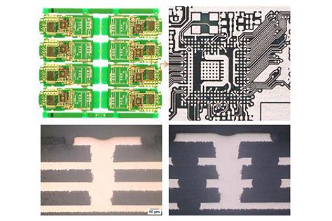
Multi-layer PCBs consist of three or more conductive layers, separated by insulating layers. The conductive layers are interconnected using PTHs or vias. As the number of layers increases, so does the complexity and cost of the PCB. However, multi-layer PCBs offer the highest design flexibility, allowing for more complex circuits and better signal integrity.
| PCB Type | Number of Conductive Layers | Complexity | Cost |
|---|---|---|---|
| Single-layer | 1 | Low | Low |
| Double-layer | 2 | Medium | Medium |
| Multi-layer | 3 or more | High | High |
Materials Used in PCB Buildup
The materials used in the PCB buildup play a crucial role in determining the board’s electrical, mechanical, and thermal properties. The most common materials used in PCB buildup include:
Substrate Materials
- FR-4: A glass-reinforced epoxy laminate, widely used for its good mechanical and electrical properties, as well as its cost-effectiveness.
- High-Frequency Materials: Specialized substrates, such as Rogers or Teflon, are used for high-frequency applications to minimize signal loss and maintain signal integrity.
- Flexible Materials: Polyimide or polyester films are used for flexible PCBs, allowing the board to bend and conform to various shapes.
Conductive Materials
- Copper: The most common conductive material used in PCBs, chosen for its excellent electrical conductivity and relatively low cost.
- Gold: Used for selective plating of connectors or exposed surfaces to improve corrosion resistance and wire bonding capabilities.
- Silver: Sometimes used as a conductive ink for printed electronics or as a surface finish for high-frequency applications.
Solder Mask
Solder mask is a protective layer applied over the copper traces, leaving only the exposed pads for soldering. It helps prevent short circuits and improves the PCB’s aesthetics. Solder masks are typically green, but other colors are available.
Silkscreen
Silkscreen is a printed layer on the PCB that provides text, logos, and component outlines for easier assembly and identification. Silkscreen is usually white, but other colors can be used.

PCB Stackup Design Considerations
When designing the PCB buildup, several factors must be considered to ensure optimal performance and manufacturability:
-
Signal Integrity: Proper layer arrangement and spacing help maintain signal integrity, minimize crosstalk, and reduce electromagnetic interference (EMI).
-
Power Distribution: Dedicated power and ground planes provide stable power distribution and reduce noise.
-
Thermal Management: Appropriate layer thickness and materials help dissipate heat generated by components.
-
Manufacturing Constraints: The PCB buildup must adhere to the manufacturing capabilities of the chosen fabrication house, considering minimum trace widths, spacing, and hole sizes.
-
Cost: The number of layers and materials used directly impact the cost of the PCB. A balance between performance and cost must be struck based on the application requirements.
PCB Buildup Manufacturing Process
The manufacturing process for PCB buildup involves several steps:
-
Inner Layer Fabrication: The conductive patterns for the inner layers are printed and etched onto the copper-clad laminates.
-
Lamination: The inner layers are stacked with insulating prepreg materials and copper foils for the outer layers. The stack is then subjected to high temperature and pressure to bond the layers together.
-
Drilling: Holes are drilled through the laminated board for PTHs, vias, and component mounting.
-
Plating: The drilled holes are plated with copper to establish electrical connections between layers.
-
Outer Layer Fabrication: The outer layer conductive patterns are printed and etched.
-
Solder Mask Application: The solder mask is applied and cured, exposing only the pads for soldering.
-
Silkscreen Printing: The silkscreen layer is printed onto the PCB for component identification and aesthetics.
-
Surface Finish: A surface finish, such as HASL, ENIG, or OSP, is applied to the exposed pads to improve solderability and protect the copper from oxidation.
Frequently Asked Questions (FAQ)
1. What is the difference between a single-layer and a double-layer PCB?
A single-layer PCB has only one conductive layer, while a double-layer PCB has two conductive layers, one on each side of the insulating substrate. Double-layer PCBs offer more design flexibility and higher component density compared to single-layer boards.
2. What materials are commonly used for PCB substrates?
The most common PCB substrate material is FR-4, a glass-reinforced epoxy laminate. For high-frequency applications, specialized substrates like Rogers or Teflon are used. Flexible PCBs use materials such as polyimide or polyester films.
3. Why are multi-layer PCBs used?
Multi-layer PCBs are used for more complex circuits that require higher component density and better signal integrity. They offer the highest design flexibility among PCB Types, allowing for more intricate routing and better noise reduction.
4. What is the purpose of solder mask on a PCB?
Solder mask is a protective layer applied over the copper traces, leaving only the exposed pads for soldering. It helps prevent short circuits, provides insulation between closely spaced traces, and improves the PCB’s aesthetics.
5. How does the number of layers affect the cost of a PCB?
As the number of layers in a PCB increases, so does the complexity and cost of the board. More layers require additional fabrication steps, materials, and processing time, leading to higher manufacturing costs. However, the improved functionality and performance of multi-layer PCBs often justify the increased cost for complex electronic devices.
Conclusion
The buildup of a PCB is a critical aspect of electronic design and manufacturing. Understanding the layers, materials, and design considerations involved in PCB buildup helps engineers create more reliable, efficient, and cost-effective electronic devices. As technology advances and electronic systems become more complex, the importance of optimizing PCB buildup will only continue to grow. By staying informed about the latest materials, manufacturing processes, and design techniques, engineers can ensure that their PCBs meet the ever-increasing demands of modern electronics.

No responses yet