Introduction to PCB Stencils
PCB stencils are an essential component in the production of high-quality printed circuit boards (PCBs). They are used to apply solder paste onto the PCB pads, ensuring precise and consistent solder paste application. This process is crucial for achieving reliable and efficient soldering of components onto the PCB.
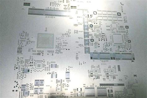
What are PCB Stencils?
PCB stencils are thin, flat sheets of metal or other materials with openings that correspond to the pads on a PCB. These openings allow solder paste to be applied to the pads in a precise and controlled manner. The stencil is placed over the PCB, and solder paste is then applied using a squeegee or automated stencil printer.
Importance of PCB Stencils in PCB Assembly
PCB stencils play a vital role in the PCB assembly process. They ensure that the correct amount of solder paste is applied to each pad, which is essential for creating reliable solder joints. Without proper solder paste application, components may not be securely attached to the PCB, leading to performance issues or even complete failure of the electronic device.
Types of PCB Stencils
There are several types of PCB stencils available, each with its own advantages and disadvantages. The choice of stencil type depends on factors such as the complexity of the PCB design, the required precision, and the production volume.
Laser-Cut Stencils
Laser-cut stencils are created using a high-precision laser cutting machine. The laser cuts the openings in the stencil material according to the PCB design. Laser-cut stencils offer high accuracy and are suitable for complex PCB designs with fine pitch components.
Advantages of laser-cut stencils:
– High precision and accuracy
– Suitable for complex PCB designs
– Durable and long-lasting
Disadvantages of laser-cut stencils:
– Higher cost compared to other stencil types
– Longer production time
Electroformed Stencils
Electroformed stencils are created using an electroplating process. A thin layer of metal, usually nickel, is deposited onto a master pattern, creating a precise replica of the PCB pads. Electroformed stencils are known for their excellent dimensional accuracy and smooth aperture walls.
Advantages of electroformed stencils:
– Excellent dimensional accuracy
– Smooth aperture walls for improved solder paste release
– Suitable for high-volume production
Disadvantages of electroformed stencils:
– Higher cost compared to laser-cut stencils
– Limited material options (usually nickel)
Chemically Etched Stencils
Chemically etched stencils are created by selectively removing material from a metal sheet using a chemical etching process. The etching process creates openings in the stencil that correspond to the PCB pads. Chemically etched stencils are less expensive than laser-cut and electroformed stencils but offer lower precision.
Advantages of chemically etched stencils:
– Lower cost compared to other stencil types
– Faster production time
– Suitable for less complex PCB designs
Disadvantages of chemically etched stencils:
– Lower precision compared to laser-cut and electroformed stencils
– Not suitable for fine pitch components or complex PCB designs

Stencil Material Options
PCB stencils can be made from various materials, each with its own properties and benefits. The choice of stencil material depends on factors such as durability, cost, and compatibility with the solder paste.
Stainless Steel Stencils
Stainless steel is the most common material used for PCB stencils. It offers excellent durability, stability, and resistance to wear and tear. Stainless steel stencils are suitable for high-volume production and can withstand multiple cleaning cycles.
Advantages of stainless steel stencils:
– Excellent durability and stability
– Suitable for high-volume production
– Resistant to wear and tear
– Compatible with most solder paste types
Disadvantages of stainless steel stencils:
– Higher cost compared to other materials
– Heavier than other materials, which may affect handling
Nickel Stencils
Nickel stencils are commonly used for electroformed stencils. They offer high precision and smooth aperture walls, which improve solder paste release. Nickel stencils are durable and suitable for high-volume production.
Advantages of nickel stencils:
– High precision and smooth aperture walls
– Excellent durability
– Suitable for high-volume production
Disadvantages of nickel stencils:
– Higher cost compared to other materials
– Limited to electroformed stencil production
Polyimide Stencils
Polyimide stencils are made from a flexible, high-temperature resistant polymer material. They are lightweight and offer good dimensional stability. Polyimide stencils are suitable for applications that require a flexible or conformable stencil.
Advantages of polyimide stencils:
– Lightweight and flexible
– Good dimensional stability
– Suitable for applications requiring a conformable stencil
Disadvantages of polyimide stencils:
– Lower durability compared to metal stencils
– Not suitable for high-volume production
– May require special handling and storage

Stencil Thickness and Aperture Design
The thickness of the stencil and the design of the apertures (openings) play a crucial role in determining the quality and consistency of solder paste deposition.
Stencil Thickness
The thickness of the stencil determines the amount of solder paste deposited onto the PCB pads. Thicker stencils deposit more solder paste, while thinner stencils deposit less. The optimal stencil thickness depends on factors such as the size of the components, the pitch of the pads, and the desired solder joint profile.
Common stencil thicknesses:
– 0.1 mm (4 mil)
– 0.12 mm (5 mil)
– 0.15 mm (6 mil)
– 0.2 mm (8 mil)
Choosing the right stencil thickness is essential for achieving the desired solder joint profile and ensuring reliable solder connections.
Aperture Design
The design of the apertures in the stencil determines the shape and size of the solder paste deposits on the PCB pads. Aperture design plays a critical role in ensuring consistent solder paste release and preventing issues such as bridging or insufficient solder paste deposition.
Factors to consider in aperture design:
– Aperture size: The size of the aperture should be appropriate for the size of the PCB pad and the component lead.
– Aperture shape: The shape of the aperture can affect solder paste release. Common shapes include square, rectangular, and circular.
– Aperture wall angle: The angle of the aperture walls can impact solder paste release. Tapered walls can improve release compared to straight walls.
Proper aperture design ensures consistent solder paste deposition and helps prevent common soldering defects.

Stencil Frame Types
PCB stencils are typically mounted in a frame to ensure stability and prevent deformation during the solder paste printing process. There are several types of stencil frames available, each with its own advantages and disadvantages.
Aluminum Frames
Aluminum frames are lightweight and cost-effective. They are suitable for low-volume production and prototyping. Aluminum frames are easy to handle and store but may not be as durable as other frame types.
Advantages of aluminum frames:
– Lightweight and easy to handle
– Cost-effective
– Suitable for low-volume production and prototyping
Disadvantages of aluminum frames:
– Lower durability compared to other frame types
– May not be suitable for high-volume production
Steel Frames
Steel frames are more durable and stable than aluminum frames. They are suitable for high-volume production and can withstand the rigors of repeated use. Steel frames offer excellent flatness and resistance to deformation.
Advantages of steel frames:
– Excellent durability and stability
– Suitable for high-volume production
– Good flatness and resistance to deformation
Disadvantages of steel frames:
– Heavier than aluminum frames
– Higher cost compared to aluminum frames
Frameless Stencils
Frameless stencils, also known as tension-mounted stencils, are stencils that are mounted directly onto the solder paste printer without the use of a frame. Frameless stencils offer several advantages, such as improved print accuracy and reduced stencil storage space.
Advantages of frameless stencils:
– Improved print accuracy due to reduced stencil deformation
– Reduced storage space requirements
– Faster changeover times between different stencils
Disadvantages of frameless stencils:
– Requires compatible solder paste printers
– May not be suitable for all PCB designs
Stencil Cleaning and Maintenance
Regular cleaning and maintenance of PCB stencils are essential for ensuring consistent solder paste printing quality and extending the lifespan of the stencils.
Stencil Cleaning Methods
There are several methods for cleaning PCB stencils, depending on the type of solder paste and the level of contamination.
- Manual cleaning: Manual cleaning involves using solvents and wiping the stencil with a lint-free cloth. This method is suitable for light contamination and low-volume production.
- Ultrasonic cleaning: Ultrasonic cleaning uses high-frequency sound waves to agitate a cleaning solution, effectively removing solder paste residue from the stencil. This method is suitable for heavy contamination and high-volume production.
- Automated cleaning: Automated cleaning systems use a combination of solvents, brushes, and air knives to clean the stencil. This method is efficient and consistent, making it suitable for high-volume production.
Regular cleaning of PCB stencils helps prevent solder paste buildup, ensures consistent print quality, and extends the lifespan of the stencils.
Stencil Storage and Handling
Proper storage and handling of PCB stencils are crucial for maintaining their quality and performance. Stencils should be stored in a clean, dry environment and protected from damage.
Tips for stencil storage and handling:
– Store stencils vertically to prevent deformation
– Use stencil storage racks or containers to protect stencils from damage
– Handle stencils with clean, lint-free gloves to avoid contamination
– Inspect stencils regularly for signs of wear or damage
Proper storage and handling of PCB stencils help ensure their longevity and maintain consistent solder paste printing quality.
Solder Paste Selection for PCB Stencils
Selecting the appropriate solder paste for use with PCB stencils is essential for achieving reliable solder joints and optimal printing performance.
Solder Paste Types
There are several types of solder paste available, each with its own characteristics and benefits.
- Lead-based solder paste: Lead-based solder pastes contain a mixture of tin and lead. They have a lower melting point and are easier to work with compared to lead-free solder pastes. However, due to environmental and health concerns, lead-based solder pastes are being phased out in many industries.
- Lead-free solder paste: Lead-free solder pastes are becoming increasingly common due to environmental regulations. They typically contain a mixture of tin, silver, and copper (SAC alloys). Lead-free solder pastes have a higher melting point and may require adjustments to the soldering process.
- No-clean solder paste: No-clean solder pastes contain flux that does not require cleaning after the soldering process. These solder pastes are suitable for applications where post-soldering cleaning is not feasible or desirable.
- Water-soluble solder paste: Water-soluble solder pastes contain flux that can be easily cleaned using water or aqueous cleaning solutions. These solder pastes are suitable for applications that require complete flux removal after soldering.
Selecting the appropriate solder paste depends on factors such as the PCB design, environmental requirements, and the desired soldering process.
Solder Paste Properties
When selecting solder paste for use with PCB stencils, several key properties should be considered.
- Viscosity: The viscosity of the solder paste determines its flow characteristics and ability to fill stencil apertures. Solder pastes with the appropriate viscosity ensure consistent solder paste deposition and prevent issues such as bridging or insufficient filling.
- Particle size: The size of the solder particles in the paste affects the printing process and the resulting solder joint quality. Smaller particle sizes allow for finer pitch components and improved printing resolution.
- Flux activity: The flux activity of the solder paste determines its ability to remove oxides and promote wetting of the solder to the PCB pads and component leads. Solder pastes with the appropriate flux activity ensure reliable solder joint formation.
Choosing solder paste with the right properties for the specific application and PCB design helps optimize the solder paste printing process and ensures reliable solder joint formation.
Advanced PCB Stencil Techniques
As PCB designs become more complex and miniaturized, advanced stencil techniques are being developed to improve solder paste printing quality and accommodate challenging components and layouts.
Step Stencils
Step stencils, also known as multi-level stencils, have different thicknesses in different areas of the stencil. This allows for the deposition of different amounts of solder paste on different components or pads. Step stencils are particularly useful for PCBs with a mix of large and small components or varying pad sizes.
Advantages of step stencils:
– Accommodate different solder paste volume requirements on a single PCB
– Improve solder joint quality for components with varying sizes
– Reduce the need for multiple stencils or print cycles
3D Stencils
3D stencils, also known as formed stencils or relief stencils, have a three-dimensional profile that allows for better control over solder paste deposition. 3D stencils can have tapered aperture walls, stepped apertures, or other complex geometries that improve solder paste release and accommodate specific component requirements.
Advantages of 3D stencils:
– Improved solder paste release and control
– Accommodate specific component requirements, such as fine pitch or small size components
– Reduce solder paste bridging and other printing defects
Nanocoatings for Stencils
Nanocoatings are ultra-thin coatings applied to the surface of the stencil to improve solder paste release and prevent solder paste adhesion. These coatings typically have a thickness of a few nanometers and are made from materials such as fluoropolymers or silicones.
Advantages of nanocoatings for stencils:
– Improve solder paste release and prevent adhesion
– Reduce the need for frequent stencil cleaning
– Extend the lifespan of the stencil
Nanocoatings can be applied to both new and existing stencils and are compatible with most solder paste types.
Quality Control and Inspection for PCB Stencils
Ensuring the quality and consistency of PCB stencils is essential for achieving reliable solder paste printing and high-quality solder joints. Quality control and inspection processes help identify and prevent issues related to stencil manufacturing, storage, and usage.
Stencil Inspection Techniques
Several inspection techniques are used to assess the quality and condition of PCB stencils.
- Visual inspection: Visual inspection involves examining the stencil for signs of damage, wear, or contamination. This can be done using magnification tools or automated optical inspection systems.
- Dimensional inspection: Dimensional inspection uses specialized measurement tools, such as microscopes or coordinate measuring machines (CMMs), to verify the accuracy of stencil aperture sizes and positions.
- Solder paste volume measurement: Solder paste volume measurement techniques, such as 3D solder paste inspection (SPI) systems, are used to assess the volume and consistency of solder paste deposits printed using the stencil.
Regular inspection of PCB stencils helps identify issues early and ensures consistent solder paste printing quality.
Stencil Quality Standards
Several industry standards provide guidelines and requirements for PCB stencil quality and performance.
- IPC-7525: Stencil Design Guidelines
- IPC-7526: Stencil Qualification and Process Control
- IPC-7527: Solder Paste Printing Troubleshooting Guide
These standards offer best practices for stencil design, qualification, and process control, helping ensure the production of high-quality PCBs.
Stencil Performance Metrics
Monitoring stencil performance metrics is essential for maintaining solder paste printing quality and identifying areas for improvement. Key stencil performance metrics include:
- Solder paste volume consistency
- Solder paste height and area
- Solder paste bridging or insufficient filling
- Stencil cleaning frequency and effectiveness
Tracking these metrics over time helps identify trends, optimize the solder paste printing process, and ensure consistent PCB Quality.
Frequently Asked Questions (FAQ)
- What is the most common material used for PCB stencils?
-
Stainless steel is the most common material used for PCB stencils due to its durability, stability, and compatibility with most solder paste types.
-
How do I choose the right stencil thickness for my PCB design?
- The optimal stencil thickness depends on factors such as component size, pad pitch, and the desired solder joint profile. Consult with your stencil manufacturer or refer to industry guidelines to determine the appropriate thickness for your specific PC
No responses yet