What is a Ball Grid Array (BGA)?
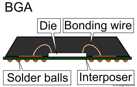
A Ball Grid Array (BGA) is a type of surface-mount packaging used for integrated circuits. It is characterized by a grid of solder balls on the bottom side of the package. These solder balls are used to conduct electrical signals from the IC to the PCB the package is mounted on.
Advantages of BGA Packages
BGA packages offer several advantages over other types of IC packaging:
| Advantage | Description |
|---|---|
| High pin count | BGAs can have hundreds or even thousands of pins, allowing for complex ICs with many inputs and outputs. |
| Small size | The ball grid array allows for a very compact package relative to the pin count. |
| Good electrical performance | The short distance between the IC and PCB and the low inductance of the solder balls provide good signal integrity and low noise. |
| Thermal performance | The grid of solder balls provides a large surface area for heat transfer away from the IC. |
Disadvantages of BGA Packages
Despite their advantages, BGA packages also have some potential drawbacks:
| Disadvantage | Description |
|---|---|
| Difficult to inspect | The solder balls are hidden under the package, making visual inspection of the solder joints difficult or impossible. |
| Hard to rework | If there is a problem with the solder joints, reworking a BGA can be challenging and requires specialized equipment. |
| Thermal expansion mismatch | If the coefficients of thermal expansion of the PCB and BGA package are not well matched, thermal cycling can stress and damage the solder joints. |
What is a Land Grid Array (LGA)?
A Land Grid Array (LGA) is another type of surface-mount packaging for ICs that is similar to a BGA. However, instead of having a grid of solder balls, an LGA has a grid of flat contact pads, called lands. The lands on the bottom of the LGA package make contact with pads on the PCB, and the IC is held in place by a clamping mechanism.
Advantages of LGA Packages
LGA packages have some advantages compared to BGAs:
| Advantage | Description |
|---|---|
| Easier inspection | With no hidden solder balls, the contact pads on an LGA are easy to visually inspect. |
| Simpler rework | If there is a problem, an LGA package can be removed and replaced more easily than a BGA. |
| Better thermal expansion matching | The clamping mechanism holds the LGA in compression against the PCB, accommodating any thermal expansion mismatch. |
Disadvantages of LGA Packages
LGAs also have some potential drawbacks compared to BGAs:
| Disadvantage | Description |
|---|---|
| Lower pin density | The flat contact pads on an LGA can’t be spaced as closely as the solder balls on a BGA, limiting the maximum pin count for a given package size. |
| Clamping mechanism required | The need for a clamping mechanism to hold the LGA in contact with the PCB adds cost and complexity compared to a BGA. |

BGA vs. LGA Comparison
Now let’s directly compare some key characteristics of BGA and LGA packages:
| Characteristic | BGA | LGA |
|---|---|---|
| Connection method | Solder balls | Flat contact pads |
| Pin density | Higher | Lower |
| Inspectability | Difficult | Easy |
| Reworkability | Challenging | Simpler |
| Thermal expansion tolerance | Lower | Higher |
| Cost | Lower | Higher |
| Clamping required | No | Yes |
As you can see, each package type has its own set of trade-offs. BGAs offer higher pin density and lower cost but are harder to inspect and rework. LGAs are easier to inspect and rework and tolerate thermal expansion mismatches better but have lower pin density and higher cost.
When to Use a BGA vs. LGA
The choice between a BGA and LGA package will depend on the specific requirements of the application. Here are some general guidelines:
Use a BGA when:
– You need the highest possible pin density for a given package size
– Cost is a primary concern
– The PCB and package materials can be matched for thermal expansion
– Inspection and rework are less critical
Use an LGA when:
– Ease of inspection and rework are important
– Thermal expansion mismatches are a concern
– A lower maximum pin count is acceptable
– The added cost of the clamping mechanism is not prohibitive

Real-World Applications
BGAs and LGAs are used in a wide range of electronic systems. Here are a few examples:
Smartphone Processors
Modern smartphone systems-on-chip (SoCs) are some of the most complex ICs in mass production, with pin counts often over 1000. The high pin density and compact size of BGA packages make them a common choice for packaging smartphone SoCs.
Server CPUs
Server-class CPUs also require high pin counts to support their many cores, memory channels, and I/O interfaces. LGA packages are often used for server CPUs to allow for easier upgrades and replacement compared to BGA. The LGA socket also provides a robust clamping mechanism to ensure reliable connections.
Field-Programmable Gate Arrays (FPGAs)
FPGAs are complex programmable logic devices that can contain millions of Logic Gates and thousands of I/O pins. High-end FPGAs often use BGA packaging to achieve the necessary pin density in a reasonable package size. However, some lower-pin-count FPGAs may use LGA packages for easier PCB Assembly and rework.

Frequently Asked Questions
1. Can a BGA package be replaced with an LGA package?
In most cases, no. BGA and LGA packages have different footprints and attachment methods, so they are not directly interchangeable. The choice of BGA or LGA needs to be made early in the PCB design process.
2. Are BGA and LGA packages the only options for surface-mount ICs?
No, there are several other types of surface-mount packages, such as Quad Flat Packages (QFP), Small Outline Packages (SOP), and Dual Flat No-Lead (DFN) packages. However, BGA and LGA packages are the most common choices for high-pin-count ICs.
3. What are the typical pin counts for BGA and LGA packages?
BGA packages can have anywhere from a few dozen to over 2000 pins, with common sizes like 256, 484, 1152, and 1924 pins. LGA packages typically have lower pin counts due to their larger contact pads, with common sizes up to around 1000 pins.
4. How are BGA and LGA packages attached to PCBs?
BGA packages are attached to the PCB by reflowing the solder balls, typically using a convection oven or vapor phase reflow process. LGA packages are clamped into a socket or compression connector which is soldered to the PCB.
5. What are some common reliability issues with BGA and LGA packages?
Some common reliability issues include solder joint fatigue due to thermal expansion mismatches, solder ball bridging or opens due to poor reflow, and pad cratering or delamination on the PCB side. Proper design, material selection, and process control are critical for reliable BGA and LGA assembly.
Conclusion
BGA and LGA packages are two of the most important packaging options for high-pin-count ICs. While they serve similar purposes, they have some key differences in terms of pin density, inspectability, reworkability, thermal expansion tolerance, and cost.
Understanding these differences is crucial when selecting a package type for a particular application. BGAs offer the highest pin densities and lowest cost but are more challenging to inspect and rework. LGAs provide easier inspection and rework and better thermal expansion tolerance but have lower pin densities and higher cost.
Regardless of which package type is chosen, careful design, material selection, and process control are essential to ensure reliable and high-performing electronic assemblies. As electronic systems continue to increase in complexity and miniaturization, innovations in BGA, LGA, and other packaging technologies will play a critical role in enabling the next generation of electronic devices.
No responses yet