What is an 8 Layer PCB?
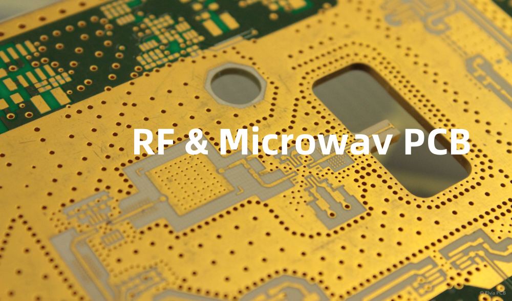
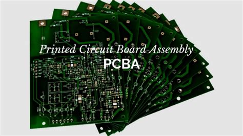
An 8 layer PCB is a printed circuit board that consists of eight conductive copper layers laminated together with insulating material. These layers are interconnected using vias, which are small holes drilled through the board and plated with conductive material. The increased number of layers allows for more complex circuit designs and higher component density compared to simpler PCBs.
Advantages of 8 Layer PCBs
- Increased functionality
- Higher component density
- Improved signal integrity
- Better heat dissipation
- Enhanced electromagnetic compatibility (EMC)
Choosing the Right 8 Layer PCB Manufacturer
When selecting an 8 layer PCB manufacturer, there are several key factors to consider to ensure you receive high-quality boards that meet your project’s requirements.
Factors to Consider
- Manufacturing capabilities
- Quality control processes
- Lead times
- Pricing
- Customer support
Top 8 Layer PCB Manufacturers
| Manufacturer | Location | Certifications | Specialties |
|---|---|---|---|
| PCBWay | China | ISO9001, UL, RoHS | Prototype and low-volume production |
| Advanced Circuits | USA | ISO9001, AS9100, ITAR | Quick-turn prototypes and high-reliability boards |
| Sunstone Circuits | USA | ISO9001, ITAR, MIL-PRF-31032 | High-quality prototypes and production runs |
| Eurocircuits | Europe | ISO9001, UL, IPC Class 2 & 3 | Prototype and medium-volume production |
8 Layer PCB Design Considerations
Designing an 8 layer PCB requires careful planning and attention to detail to ensure optimal performance and manufacturability.
Key Design Aspects
- Layer stackup
- Via placement and size
- Trace width and spacing
- Component placement
- Signal integrity and EMC
Best Practices for 8 Layer PCB Design
- Use a consistent layer stackup
- Minimize via count and optimize placement
- Follow manufacturer’s design guidelines
- Perform signal integrity simulations
- Implement proper grounding and shielding techniques

8 Layer PCB Manufacturing Process
The manufacturing process for 8 layer PCBs involves several steps to ensure the highest quality and reliability.
Manufacturing Steps
- Material selection and preparation
- Inner layer printing and etching
- Lamination
- Drilling
- Plating
- Outer layer printing and etching
- Solder mask application
- Surface finish application
- Electrical testing and inspection
Quality Control in 8 Layer PCB Manufacturing
- Automated optical inspection (AOI)
- X-ray inspection
- Electrical testing
- Visual inspection
- Destructive testing
Applications of 8 Layer PCBs
8 layer PCBs are used in a wide range of industries and applications where high performance, reliability, and functionality are crucial.
Industries Using 8 Layer PCBs
- Aerospace and defense
- Medical devices
- Automotive electronics
- Industrial automation
- Telecommunications
Examples of 8 Layer PCB Applications
- Satellite communication systems
- Medical imaging equipment
- Advanced driver assistance systems (ADAS)
- Industrial control systems
- 5G network infrastructure
8 Layer PCB Cost Factors
The cost of 8 layer PCBs depends on several factors, including the complexity of the design, the materials used, and the manufacturing process.
Factors Affecting 8 Layer PCB Cost
- Board size and thickness
- Number of unique parts and components
- Material selection
- Surface finish
- Quantity ordered
Cost Reduction Strategies for 8 Layer PCBs
- Optimize board size and layout
- Minimize unique parts and components
- Choose cost-effective materials
- Consider alternative surface finishes
- Order in larger quantities
Future Trends in 8 Layer PCB Manufacturing
As technology continues to advance, 8 layer PCB manufacturers are adopting new materials, processes, and technologies to meet the evolving needs of their customers.
Emerging Trends in 8 Layer PCB Manufacturing
- High-frequency materials
- Embedded components
- 3D printing
- Flexible and Rigid-flex PCBs
- Eco-friendly materials and processes
Impact of Industry 4.0 on 8 Layer PCB Manufacturing
- Automation and robotics
- Internet of Things (IoT) integration
- Big data analytics
- Artificial intelligence and machine learning
- Digital twin technology
Frequently Asked Questions (FAQ)
- What is the typical turnaround time for 8 layer PCBs?
-
The turnaround time for 8 layer PCBs varies depending on the manufacturer and the complexity of the design. Typically, prototype quantities can be produced within 5-10 business days, while larger production runs may take 2-4 weeks.
-
Can 8 layer PCBs be manufactured with impedance control?
-
Yes, 8 layer PCBs can be manufactured with impedance control. This is achieved by carefully controlling the trace width, spacing, and dielectric thickness to maintain a specific characteristic impedance throughout the board.
-
What is the minimum feature size for 8 layer PCBs?
-
The minimum feature size for 8 layer PCBs depends on the manufacturer’s capabilities. Most manufacturers can achieve a minimum trace width and spacing of 3-4 mils (0.075-0.1 mm) on inner layers and 4-5 mils (0.1-0.125 mm) on outer layers.
-
How do I choose the right surface finish for my 8 layer PCB?
-
The choice of surface finish depends on the application, the components used, and the environmental conditions the PCB will be exposed to. Common surface finishes for 8 layer PCBs include ENIG (Electroless Nickel Immersion Gold), HASL (Hot Air Solder Leveling), and OSP (Organic Solderability Preservative).
-
Can 8 layer PCBs be manufactured with blind and buried vias?
- Yes, 8 layer PCBs can be manufactured with blind and buried vias. Blind vias connect an outer layer to an inner layer, while buried vias connect two or more inner layers without reaching the outer layers. These advanced via types can help reduce board size and improve signal integrity.
Conclusion
8 layer PCBs offer a high level of functionality, performance, and reliability for advanced electronic applications. When choosing an 8 layer PCB manufacturer, it’s essential to consider factors such as manufacturing capabilities, quality control processes, and customer support to ensure the best possible results. By understanding the design considerations, manufacturing process, and cost factors associated with 8 layer PCBs, you can make informed decisions and create high-quality, reliable electronic products.

No responses yet