Introduction to the 74LS74 Dual Flip-flop
The 74LS74 is a widely used integrated circuit (IC) that contains two independent positive-edge-triggered D-type flip-flops. This versatile device is part of the 7400 series of logic ICs and is known for its reliability, speed, and low power consumption. The 74LS74 is commonly used in various digital circuits, such as counters, shift registers, and synchronous control systems.
In this comprehensive guide, we will explore the features, functionalities, and applications of the 74LS74 dual flip-flop. We will also provide practical examples and answer frequently asked questions to help you better understand and utilize this essential component in your digital designs.
Understanding the Basics of Flip-flops
Before diving into the specifics of the 74LS74, let’s review the fundamentals of flip-flops. A flip-flop is a digital circuit that can store a single bit of information. It has two stable states, typically referred to as “set” (or “1”) and “reset” (or “0”). Flip-flops are essential building blocks in sequential logic circuits, where the output depends not only on the current inputs but also on the previous state of the circuit.
There are several types of flip-flops, each with its own characteristics and triggering methods:
- SR (Set-Reset) Flip-flop
- D (Data) Flip-flop
- JK Flip-flop
- T (Toggle) Flip-flop
The 74LS74 is a dual D-type flip-flop, which means it has two independent flip-flops that store data based on the state of the D input at the rising edge of the clock signal.

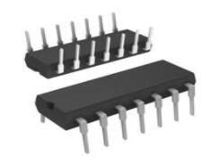
Pin Configuration and Function Table
The 74LS74 comes in a 14-pin dual in-line package (DIP). The pin configuration and function table are as follows:
| Pin Number | Pin Name | Function |
|---|---|---|
| 1 | CLR1 | Clear input for flip-flop 1 (active low) |
| 2 | D1 | Data input for flip-flop 1 |
| 3 | CLK1 | Clock input for flip-flop 1 |
| 4 | PRE1 | Preset input for flip-flop 1 (active low) |
| 5 | Q1 | Output of flip-flop 1 |
| 6 | !Q1 | Complementary output of flip-flop 1 |
| 7 | GND | Ground |
| 8 | !Q2 | Complementary output of flip-flop 2 |
| 9 | Q2 | Output of flip-flop 2 |
| 10 | PRE2 | Preset input for flip-flop 2 (active low) |
| 11 | CLK2 | Clock input for flip-flop 2 |
| 12 | D2 | Data input for flip-flop 2 |
| 13 | CLR2 | Clear input for flip-flop 2 (active low) |
| 14 | VCC | Power supply (+5V) |

Functional Description
The 74LS74 operates as follows:
- When the CLK input transitions from low to high (rising edge), the state of the D input is transferred to the Q output.
- If the PRE input is low, the Q output is forced high (logic “1”), regardless of the state of the other inputs.
- If the CLR input is low, the Q output is forced low (logic “0”), regardless of the state of the other inputs.
- If both PRE and CLR inputs are low simultaneously, the output state is undefined.
The truth table for the 74LS74 is:
| PRE | CLR | CLK | D | Q | !Q |
|---|---|---|---|---|---|
| L | H | X | X | H | L |
| H | L | X | X | L | H |
| L | L | X | X | ? | ? |
| H | H | ↑ | L | L | H |
| H | H | ↑ | H | H | L |
| H | H | L | X | Q0 | !Q0 |
Note: L = Low, H = High, X = Don’t care, ↑ = Rising edge, ? = Undefined, Q0 = Previous state of Q

Applications and Examples
The 74LS74 dual flip-flop finds applications in various digital circuits, such as:
- Frequency Dividers
- By connecting the !Q output to the D input, the 74LS74 can function as a divide-by-2 frequency divider.
-
Multiple 74LS74s can be cascaded to create divide-by-4, divide-by-8, or higher-order frequency dividers.
-
Shift Registers
- The 74LS74 can be used to create shift registers by connecting multiple flip-flops in series.
-
Data is shifted from one flip-flop to the next on each clock pulse, allowing for serial-to-parallel or parallel-to-serial data conversion.
-
Counters
- The 74LS74 can be configured as a binary counter by connecting the !Q output of one flip-flop to the CLK input of the next flip-flop.
-
Ripple counters and synchronous counters can be implemented using the 74LS74.
-
Synchronous Control Systems
- The 74LS74 can be used to synchronize asynchronous signals to a common clock domain, preventing metastability issues.
- It can also be used to generate control signals and manage the timing of various operations in a digital system.
Interfacing with the 74LS74
When incorporating the 74LS74 into your digital designs, consider the following:
- Power Supply
- The 74LS74 requires a +5V power supply, which is connected to the VCC pin (pin 14).
-
The GND pin (pin 7) should be connected to the common ground of your circuit.
-
Input and Output Connections
- Connect the appropriate signals to the D, CLK, PRE, and CLR inputs of each flip-flop.
-
The Q and !Q outputs can be connected to other parts of your circuit as required.
-
Timing Considerations
- Ensure that the setup and hold times for the D input with respect to the rising edge of the CLK input are met to avoid metastability issues.
- Consider the propagation delays of the 74LS74 when designing your circuit’s timing.
Frequently Asked Questions (FAQ)
- What is the difference between the 74LS74 and the 74HC74?
- The 74LS74 is part of the Low-power Schottky TTL (LS-TTL) family, while the 74HC74 belongs to the High-speed CMOS (HC) family.
-
The 74HC74 has lower power consumption and can operate at higher frequencies compared to the 74LS74.
-
Can the 74LS74 be used as a latch?
-
Yes, by connecting the D input to the Q output and using the PRE and CLR inputs as enable signals, the 74LS74 can function as a transparent latch.
-
How can I cascade multiple 74LS74s to create a larger shift register?
- Connect the Q output of one flip-flop to the D input of the next flip-flop in the chain.
-
Use a common clock signal for all the flip-flops to ensure synchronous operation.
-
What is the maximum clock frequency that the 74LS74 can handle?
- The maximum clock frequency depends on the specific version of the 74LS74 and the operating conditions.
-
Typically, the 74LS74 can operate at clock frequencies up to 25 MHz.
-
How do I prevent metastability issues when using the 74LS74?
- Ensure that the setup and hold times for the D input with respect to the rising edge of the CLK input are met.
- Use synchronization techniques, such as double-flop synchronizers, when interfacing asynchronous signals with the 74LS74.
Conclusion
The 74LS74 dual flip-flop is a versatile and widely used component in digital electronics. Its ability to store and synchronize data makes it an essential building block in various applications, such as frequency dividers, shift registers, counters, and control systems.
By understanding the pin configuration, functionality, and applications of the 74LS74, you can effectively incorporate this device into your digital designs. Remember to consider factors such as power supply, input/output connections, and timing requirements to ensure proper operation and reliability.
With this comprehensive guide, you now have a solid foundation to explore further possibilities and create innovative digital circuits using the 74LS74 dual flip-flop.
No responses yet