Introduction to USB PCB
USB (Universal Serial Bus) is a widely used standard for connecting peripherals to computers and other electronic devices. USB PCBs (Printed Circuit Boards) are the physical boards that contain the circuitry and components necessary for USB communication. These PCBs play a crucial role in enabling the functionality and reliability of USB devices.
However, designing and manufacturing USB PCBs can present various challenges and problems. In this article, we will explore the common issues encountered during USB PCB development and provide solutions to overcome them.
Common Problems with USB PCBs
Signal Integrity Issues
One of the primary challenges in USB PCB design is maintaining signal integrity. USB signals are high-speed and susceptible to electromagnetic interference (EMI) and crosstalk. Poor signal integrity can lead to data corruption, communication errors, and device malfunctions.
To address signal integrity issues, consider the following solutions:
– Use controlled impedance traces: Ensure that the PCB traces have the correct impedance to match the USB specification. This helps minimize reflections and signal distortions.
– Implement proper grounding: Provide a solid ground plane and use ground stitching techniques to reduce ground bounce and minimize EMI.
– Route signals carefully: Keep USB traces as short as possible and avoid sharp bends or crossing over other signals. Maintain appropriate spacing between traces to minimize crosstalk.
– Use differential pair routing: USB signals are transmitted as differential pairs. Route the positive and negative signals together with equal length and spacing to maintain signal integrity.
Power Management Challenges
USB devices often require specific power requirements, such as voltage levels and current ratings. Inefficient power management can lead to device failures, overheating, and reduced performance.
To tackle power management challenges, consider the following solutions:
– Use appropriate voltage regulators: Select voltage regulators with the correct output voltage and current ratings to meet the USB device’s power requirements.
– Implement proper decoupling: Place decoupling capacitors close to the power pins of USB ICs to minimize noise and ensure stable power supply.
– Consider power sequencing: If multiple voltages are required, ensure proper power sequencing to avoid device damage during power-up and power-down.
– Optimize power distribution: Use wide power traces and multiple power planes to minimize voltage drops and ensure even power distribution across the PCB.
ESD Protection
USB devices are prone to electrostatic discharge (ESD) events, which can damage sensitive electronic components and cause device failures.
To protect USB PCBs from ESD, consider the following solutions:
– Incorporate ESD protection devices: Use ESD protection components, such as transient voltage suppressors (TVS) or ESD diodes, on the USB data lines and power lines.
– Implement proper grounding: Provide a low-impedance path for ESD currents to discharge safely to ground. Use dedicated ESD ground planes and connect them to the main ground plane.
– Follow ESD-safe handling procedures: During manufacturing and assembly, ensure that proper ESD-safe handling procedures are followed, such as using grounded wrist straps and ESD-safe workstations.
Mechanical Challenges
USB connectors and receptacles are subject to mechanical stresses during insertion and removal. Poor mechanical design can lead to connector damage, loose connections, and reduced reliability.
To address mechanical challenges, consider the following solutions:
– Choose reliable connectors: Select USB connectors from reputable manufacturers that meet the USB specification and have proven reliability.
– Provide proper mechanical support: Use reinforced connector mounting techniques, such as through-hole mounting or additional support structures, to prevent connector damage.
– Consider strain relief: Implement strain relief mechanisms, such as cable clamps or housing features, to reduce mechanical stress on the USB connectors.
– Conduct thorough mechanical testing: Perform rigorous mechanical testing, including insertion/removal cycles and vibration tests, to ensure the USB PCB can withstand real-world usage conditions.

Best Practices for USB PCB Design
To minimize problems and ensure optimal performance of USB PCBs, follow these best practices:
-
Adhere to USB specifications: Familiarize yourself with the USB specification relevant to your design (USB 2.0, USB 3.0, etc.) and follow the guidelines for electrical and mechanical requirements.
-
Use high-quality components: Select USB controllers, transceivers, and connectors from reputable manufacturers that meet the USB specification and have a proven track record of reliability.
-
Implement proper layout techniques: Follow good PCB layout practices, such as minimizing trace lengths, avoiding sharp bends, providing sufficient clearances, and using ground planes effectively.
-
Conduct thorough simulations: Perform signal integrity simulations and power integrity analysis to identify and address potential issues early in the design phase.
-
Perform comprehensive testing: Conduct rigorous testing of the USB PCB, including functional testing, compliance testing, and environmental testing, to ensure its reliability and performance.
-
Consider manufacturing considerations: Collaborate closely with the PCB manufacturer to ensure manufacturability, select appropriate materials, and specify the required manufacturing processes and tolerances.

Troubleshooting USB PCB Issues
Despite following best practices, issues may still arise during USB PCB development. Here are some troubleshooting tips:
-
Check connectivity: Verify that all connections are properly soldered and there are no shorts or open circuits. Use a multimeter or Continuity Tester to check for connectivity issues.
-
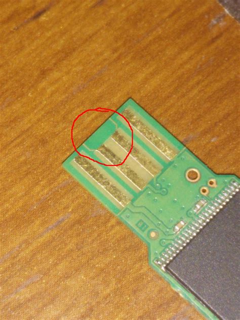
Inspect visual defects: Visually inspect the PCB for any defects, such as damaged traces, lifted pads, or solder bridges. Use magnification tools if necessary.
-
Analyze signal waveforms: Use an oscilloscope to analyze USB signal waveforms and check for signal integrity issues, such as excessive ringing, overshoot, or undershoot.
-
Verify power supply: Measure the voltage levels at relevant points on the PCB to ensure they meet the USB specification. Check for any voltage drops or fluctuations.
-
Isolate the problem: If the issue persists, systematically isolate the problem by testing individual components or sections of the PCB. This helps narrow down the root cause of the issue.
-
Consult community resources: Engage with online forums, discussion groups, or USB-specific communities to seek advice and insights from experienced designers and engineers.

FAQ
- What are the most common causes of USB PCB failures?
-
Poor signal integrity, inadequate power management, lack of ESD protection, and mechanical stress are among the most common causes of USB PCB failures.
-
How can I ensure signal integrity in my USB PCB design?
-
To ensure signal integrity, use controlled impedance traces, implement proper grounding techniques, route signals carefully, and use differential pair routing for USB signals.
-
What are the power management considerations for USB PCBs?
-
Use appropriate voltage regulators, implement proper decoupling, consider power sequencing, and optimize power distribution to ensure efficient power management in USB PCBs.
-
How can I protect my USB PCB from ESD damage?
-
Incorporate ESD protection devices, implement proper grounding, and follow ESD-safe handling procedures during manufacturing and assembly to protect USB PCBs from ESD damage.
-
What should I do if I encounter issues with my USB PCB?
- If you encounter issues with your USB PCB, check connectivity, inspect for visual defects, analyze signal waveforms, verify power supply, isolate the problem, and consult community resources for troubleshooting assistance.
Conclusion
Designing and manufacturing USB PCBs can present various challenges and problems. By understanding the common issues related to signal integrity, power management, ESD protection, and mechanical aspects, engineers can take proactive measures to mitigate these problems.
Following best practices, such as adhering to USB specifications, using high-quality components, implementing proper layout techniques, conducting thorough simulations and testing, and considering manufacturing considerations, can greatly minimize the occurrence of USB PCB issues.
When problems do arise, systematic troubleshooting approaches, including connectivity checks, visual inspections, signal analysis, power supply verification, and problem isolation, can help identify and resolve the root causes efficiently.
By addressing the challenges head-on and implementing effective solutions, engineers can ensure the reliability, performance, and success of their USB PCB designs.
No responses yet