Introduction to Logic Probes
A logic probe is an essential tool for troubleshooting and analyzing digital circuits. It allows you to quickly determine the logic state (high or low) of a digital signal, as well as detect pulses and oscillations. While commercial logic probes are readily available, building your own DIY Logic Probe can be a fun and educational project. In this comprehensive guide, we will walk you through the step-by-step process of creating your own logic probe from scratch.
What is a Logic Probe?
A logic probe is a handheld device that helps in testing and debugging digital circuits by indicating the logic state of a signal. It typically has a pointy tip that can be touched to a circuit node, and LED indicators to display the logic level (high or low) of the signal at that point. Some advanced logic probes may also have additional features such as pulse detection, audible feedback, or adjustable thresholds.
Why Build Your Own Logic Probe?
Building your own logic probe has several advantages:
-
Cost-effective: Commercial logic probes can be expensive, especially for hobbyists or students. Making your own probe is much more affordable.
-
Customization: By building your own probe, you can customize it to your specific needs and preferences. You can choose the features, indicators, and even the enclosure design.
-
Learning opportunity: The process of designing and assembling a logic probe is a great way to learn about digital circuits, components, and tools. It provides hands-on experience and deepens your understanding of electronics.
-
Satisfaction: There’s a certain sense of pride and accomplishment that comes from using a tool you’ve built yourself. It’s a rewarding experience to see your creation in action.
Components and Tools Required
Before we dive into the construction process, let’s gather all the necessary components and tools. Here’s what you’ll need:
Components
- 1x High-speed comparator IC (e.g., LM339, LM393)
- 3x Resistors (1kΩ, 10kΩ, 100kΩ)
- 2x LEDs (red and green)
- 1x Schottky diode (e.g., 1N5817, 1N5819)
- 1x Tactile switch
- 1x 9V battery connector
- 1x 9V battery
- Hook-up wires
- Prototype PCB or perfboard
- Enclosure (optional)
Tools
- Soldering iron and solder
- Wire cutters and strippers
- Multimeter
- Breadboard (for prototyping)
- Drill or hole punch (for enclosure)
- Screwdriver
- Pliers

Circuit Design and Schematic
The core of the logic probe is a high-speed comparator IC, such as the LM339 or LM393. The comparator compares the input signal to a reference voltage and outputs a high or low state based on the comparison. The schematic diagram below shows the basic circuit design:
[Insert schematic diagram image here]
The key components of the circuit are:
-
Comparator IC: It compares the input signal to the reference voltages and drives the LED indicators.
-
Input protection diode: A Schottky diode is used to protect the probe from negative voltages or accidental reverse polarity.
-
Pull-down resistor: A high-value resistor (100kΩ) is connected between the input and ground to ensure a defined state when the probe is not connected.
-
Reference voltage divider: Two resistors (1kΩ and 10kΩ) form a voltage divider to set the reference voltages for the comparator. The values are chosen to detect TTL logic levels (0-0.8V for low, 2-5V for high).
-
LED indicators: Red and green LEDs are used to indicate the logic state (red for high, green for low). Current-limiting resistors are used to protect the LEDs.
-
Power switch: A tactile switch is included to turn the probe on and off, conserving battery life when not in use.

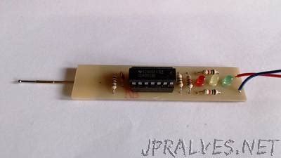
PCB Layout and Assembly
Once you have finalized the schematic, it’s time to transfer the design to a physical PCB or perfboard. Here are the steps to lay out and assemble the circuit:
-
Create a PCB layout: Use a PCB design software or draw the layout by hand on a piece of paper. Make sure to consider component placement, trace routing, and hole locations.
-
Prepare the PCB: If using a prototype PCB, solder the required components and jumper wires according to your layout. If using a perfboard, plan the component placement and drill holes for mounting.
-
Solder the components: Start by soldering the passive components (resistors and diodes), followed by the IC socket (if using one). Next, solder the LEDs, switch, and battery connector. Double-check the orientation of polarized components like LEDs and diodes.
-
Inspect and test: Carefully inspect your soldering for any bridges or poor connections. Use a multimeter to verify continuity and check for shorts. Power on the circuit and test its functionality with known logic levels.

Enclosure and Final Assembly
To make your logic probe durable and portable, you can house it in a suitable enclosure. Here’s how:
-
Choose an enclosure: Select a small plastic or metal enclosure that can fit your PCB and battery. You can repurpose a case from an old electronics project or purchase one specifically designed for projects.
-
Prepare the enclosure: Drill or punch holes in the enclosure for the probe tip, LEDs, switch, and any other necessary openings. Make sure the holes align with your PCB layout.
-
Mount the PCB: Secure the PCB inside the enclosure using screws, standoffs, or adhesive. Ensure that the probe tip, LEDs, and switch protrude through their respective holes.
-
Connect the battery: Attach the battery connector to the PCB and secure the battery inside the enclosure. You can use Battery Holders or clips to keep the battery in place.
-
Final assembly: Close the enclosure and secure it with screws or snap-fits. Attach any labels or markings as desired.
Testing and Using Your Logic Probe
With your DIY logic probe assembled, it’s time to put it to the test. Here’s how to use your probe:
-
Power on: Flip the power switch to turn on your logic probe. The LEDs may briefly flash or light up, indicating that the probe is ready.
-
Connect to circuit: Touch the probe tip to the point in the circuit you want to test. Make sure the circuit is powered on and operating.
-
Observe the LEDs: The red LED indicates a high logic state (usually 2-5V), while the green LED indicates a low state (usually 0-0.8V). If both LEDs are off, it means the signal is floating or not connected.
-
Interpret the results: Based on the LED indications, you can determine the logic state of the signal at the probed point. This information can help you diagnose issues, verify connections, or analyze circuit behavior.
-
Troubleshoot: If the probe is not functioning as expected, double-check your connections, component orientation, and soldering. Verify that the battery is fresh and supplying the correct voltage.
Advanced Features and Modifications
While the basic logic probe design is sufficient for most purposes, you can enhance its functionality with additional features and modifications. Here are a few ideas:
-
Pulse detection: Add a pulse detection circuit using a monostable multivibrator (e.g., 74HC123) to detect and indicate short pulses or glitches.
-
Audible feedback: Include a piezo buzzer or speaker to provide audible feedback for logic states or pulses. This can be helpful when probing hard-to-see points or working in noisy environments.
-
Adjustable thresholds: Replace the fixed voltage divider with a potentiometer to allow adjustable threshold levels. This enables testing of different logic families (e.g., CMOS) or detecting specific voltage levels.
-
Frequency Counter: Integrate a frequency counter circuit to measure and display the frequency of the probed signal. This can be useful for analyzing clock signals or oscillators.
-
Miniaturization: Redesign the circuit using surface-mount components (SMD) to make the probe more compact and portable. This may require advanced soldering skills and tools.
| Feature | Benefit |
|---|---|
| Pulse detection | Detect and indicate short pulses or glitches |
| Audible feedback | Provide audible indication of logic states or pulses |
| Adjustable thresholds | Enable testing of different logic families or voltages |
| Frequency counter | Measure and display the frequency of the probed signal |
| Miniaturization | Make the probe more compact and portable |
FAQ
1. Can I use this logic probe on any digital circuit?
Yes, this logic probe is designed to work with most common digital circuits, including TTL and CMOS logic. However, always ensure that the circuit’s voltage levels are within the probe’s specifications to avoid damage.
2. What is the maximum input voltage the probe can handle?
The maximum input voltage is determined by the comparator IC and the power supply. With a 9V battery, the probe can typically handle input voltages up to 5V. For higher voltages, you may need to modify the circuit or use a different comparator.
3. How long will the battery last?
The battery life depends on factors such as the comparator IC, LED current, and usage frequency. With a typical 9V alkaline battery and moderate usage, the probe should last for several hours of continuous operation. You can extend the battery life by using low-current LEDs or adding a power-saving feature.
4. Can I use this probe to detect analog signals?
No, this logic probe is designed specifically for digital signals with distinct high and low states. It cannot accurately measure or interpret analog signals, which have continuous voltage levels.
5. How do I calibrate the probe’s thresholds?
The probe’s thresholds are determined by the reference voltage divider (1kΩ and 10kΩ resistors). If you need to adjust the thresholds, you can change the resistor values according to the desired voltage levels. Use Ohm’s law to calculate the appropriate resistor values for your specific requirements.
Conclusion
Building your own DIY logic probe is a rewarding and educational project that provides a valuable tool for troubleshooting and analyzing digital circuits. By following this step-by-step guide, you can create a functional and customizable logic probe using readily available components and tools.
Remember to always prioritize safety, double-check your connections, and test your probe on known circuits before using it on critical applications. With practice and experience, you’ll become proficient in using your logic probe to diagnose and debug digital systems.
Happy probing and enjoy exploring the world of digital electronics with your own DIY logic probe!
No responses yet