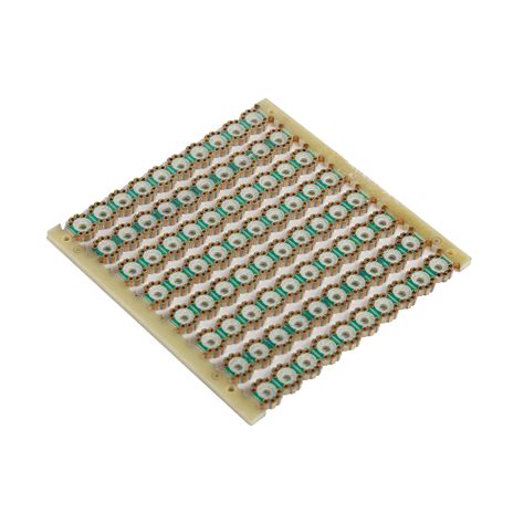
What is a Castellated PCB?
A castellated PCB, also known as a castellated printed circuit board or castellated hole PCB, is a type of circuit board that features small, semi-circular holes or slots along its edges. These holes, called castellations, serve as a unique connection point for attaching the PCB to other boards or components without the need for additional connectors or wires.
The term “castellated” derives from the resemblance of these holes to the battlements or castellations found on medieval castle walls. This distinctive design offers several advantages over traditional PCB connection methods, making castellated PCBs an increasingly popular choice for various electronic applications.
How Are Castellated Holes Created?
Castellated holes are typically created during the PCB manufacturing process using a specialized drilling technique. The process involves the following steps:
-
PCB Design: The PCB layout is designed with the castellated holes incorporated along the edges of the board. The size, spacing, and placement of these holes are carefully considered to ensure proper connectivity and mechanical stability.
-
Drilling: Once the PCB design is finalized, the board undergoes the drilling process. A computer-controlled drill machine creates the castellated holes along the edges of the board according to the specified design. The drill bit used for this process has a unique shape that creates the semi-circular profile of the castellations.
-
Plating: After drilling, the castellated holes are plated with a conductive material, typically copper, to ensure electrical connectivity. This plating process also helps to reinforce the mechanical strength of the castellations.
-
Finishing: The PCB then undergoes various finishing processes, such as solder mask application and surface finishing, to protect the board and enhance its overall durability.
Advantages of Castellated PCBs
Castellated PCBs offer several advantages over traditional PCB connection methods, such as through-hole or surface-mount connectors:
-
Space Savings: By eliminating the need for additional connectors, castellated PCBs allow for a more compact design. This is particularly beneficial in applications where space is limited, such as in wearable devices or small electronic gadgets.
-
Cost Reduction: Castellated PCBs can help reduce overall manufacturing costs by simplifying the assembly process. Without the need for separate connectors, fewer components are required, leading to lower material costs and reduced assembly time.
-
Improved Reliability: Castellated connections provide a robust and reliable means of attaching PCBs to other boards or components. The direct board-to-board connection eliminates potential points of failure associated with traditional connectors, such as loose or broken pins.
-
Enhanced Signal Integrity: The direct connection provided by castellated holes minimizes signal loss and interference compared to using separate connectors. This is particularly important in high-frequency or sensitive applications where maintaining signal integrity is crucial.
-
Flexibility in Design: Castellated PCBs offer greater flexibility in terms of board layout and orientation. They allow for perpendicular or parallel board stacking, enabling more creative and efficient designs.
Applications of Castellated PCBs
Castellated PCBs find applications in various industries and electronic devices, such as:
-
Wearable Technology: Smartwatches, fitness trackers, and other wearable devices often utilize castellated PCBs to achieve compact and lightweight designs.
-
Internet of Things (IoT): IoT devices, such as sensors and smart home appliances, frequently employ castellated PCBs for their space-saving and cost-effective properties.
-
Automotive Electronics: In-vehicle electronic systems, like infotainment displays and control modules, may use castellated PCBs to reduce weight and optimize space utilization.
-
Medical Devices: Compact medical devices, such as implantable sensors or monitoring systems, can benefit from the reliable and space-efficient connections provided by castellated PCBs.
-
Consumer Electronics: Various consumer electronic products, like smartphones, tablets, and handheld gaming devices, may incorporate castellated PCBs to achieve slim and compact designs.

Designing with Castellated PCBs
When designing a castellated PCB, several factors should be considered to ensure optimal performance and reliability:
Castellation Size and Spacing
The size and spacing of the castellated holes are crucial for proper connectivity and mechanical stability. The dimensions of the castellations should be carefully chosen based on the specific requirements of the application, such as the board thickness, component sizes, and manufacturing capabilities.
Typically, castellated holes range from 0.5mm to 2.0mm in diameter, with a pitch (distance between the centers of adjacent holes) of 1.0mm to 2.54mm. However, these dimensions can vary depending on the specific design and manufacturing constraints.
Board Thickness
The thickness of the PCB is another important consideration when designing with castellated holes. Thinner boards may require smaller castellation sizes to maintain mechanical integrity, while thicker boards can accommodate larger castellations.
Common PCB thicknesses for castellated designs range from 0.4mm to 1.6mm, although thicker boards can be used in certain applications.
Solder Mask and Pad Design
The solder mask and pad design around the castellated holes play a crucial role in ensuring proper solderability and connection reliability. The solder mask should be designed to expose the necessary amount of copper around the castellations for effective soldering.
Pad sizes and shapes should be optimized to provide sufficient area for solder joint formation while considering the specific requirements of the assembly process, such as the type of solder paste and reflow profile.
Assembly Considerations
When assembling castellated PCBs, several factors should be taken into account to ensure a successful and reliable connection:
-
Solder Paste Application: The solder paste should be applied evenly and in the appropriate amount to the castellated holes. Stencil printing or dispensing techniques can be used, depending on the volume and complexity of the assembly.
-
Component Placement: The mating board or component should be accurately aligned with the castellated holes to ensure proper connection. Specialized fixtures or automated placement equipment may be used to achieve precise alignment.
-
Reflow Soldering: The assembled boards undergo a reflow soldering process to form the solder joints between the castellated holes and the mating components. The reflow profile should be carefully controlled to ensure optimal solder joint formation and to minimize the risk of defects, such as bridging or insufficient wetting.
-
Inspection and Testing: After the reflow soldering process, the assembled boards should be visually inspected and electrically tested to verify the integrity of the castellated connections. Automated optical inspection (AOI) systems and in-circuit testing (ICT) techniques can be employed for this purpose.

Frequently Asked Questions (FAQ)
-
Q: Can castellated PCBs be used with surface-mount components?
A: Yes, castellated PCBs are compatible with surface-mount components. The castellated holes can be used to attach the PCB to another board, while the surface-mount components can be placed and soldered on the PCB’s surface using conventional SMT assembly processes. -
Q: Are castellated PCBs suitable for high-density designs?
A: Castellated PCBs can be used in high-density designs, as the castellated holes offer a compact and space-efficient means of connecting boards. However, the size and spacing of the castellations should be carefully considered to ensure compatibility with the specific design requirements and manufacturing capabilities. -
Q: Can castellated PCBs be used in harsh environmental conditions?
A: Castellated PCBs can be designed to withstand harsh environmental conditions, such as extreme temperatures, vibrations, or moisture. Proper material selection, surface finishes, and conformal coatings can be employed to enhance the durability and reliability of the PCB in challenging environments. -
Q: Are there any limitations to using castellated PCBs?
A: While castellated PCBs offer many benefits, there are a few limitations to consider. The castellated holes may not be suitable for applications requiring very high current carrying capacity, as the limited contact area of the castellations may restrict current flow. Additionally, the mechanical strength of the castellated connections may be lower compared to some traditional connector types, particularly in applications subject to high mechanical stress or vibrations. -
Q: Can castellated PCBs be reworked or repaired?
A: Reworking or repairing castellated PCBs can be more challenging compared to traditional connector-based designs. If a castellated connection is damaged or fails, it may be difficult to access and repair without affecting the surrounding components or board integrity. Proper design, assembly, and handling practices should be followed to minimize the need for rework or repair.

Conclusion
Castellated PCBs offer a unique and advantageous solution for connecting boards and components in various electronic applications. By eliminating the need for separate connectors, castellated PCBs enable more compact, cost-effective, and reliable designs.
When designing and assembling castellated PCBs, careful consideration should be given to factors such as castellation size and spacing, board thickness, solder mask and pad design, and assembly processes to ensure optimal performance and reliability.
As electronic devices continue to miniaturize and require more efficient interconnect solutions, castellated PCBs are poised to play an increasingly important role in shaping the future of PCB design and assembly.
No responses yet