Introduction to PCBs
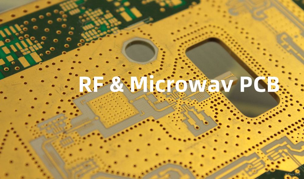
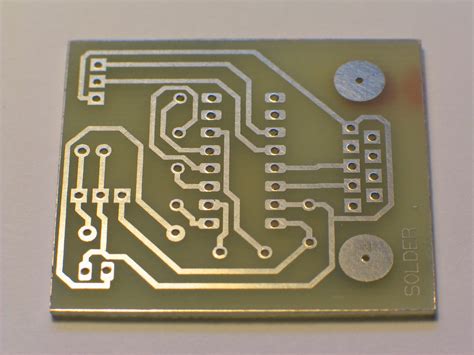
Printed Circuit Boards (PCBs) are the backbone of modern electronics. These boards are used in almost every electronic device we use today, from smartphones and laptops to medical equipment and aerospace technology. PCBs are designed to mechanically support and electrically connect electronic components using conductive tracks, pads, and other features etched from copper sheets laminated onto a non-conductive substrate.
Types of PCBs
PCBs can be classified based on the number of layers they have. The most common types are:
| Type | Layers | Description |
|---|---|---|
| Single-sided | 1 | Components are mounted on one side of the board |
| Double-sided | 2 | Components are mounted on both sides of the board |
| Multi-layer | 4+ | Multiple layers of conductive material separated by insulation |
As technology advances, the demand for more complex and compact electronic devices increases. This has led to the development of high-density interconnect (HDI) PCBs, which can accommodate a larger number of components in a smaller space. One such example is the 32-layer PCB.
What are 32 Layer PCBs?
A 32-layer PCB is a multi-layer board that consists of 32 layers of conductive material, typically copper, separated by insulating layers. These boards are designed to handle highly complex circuits and provide superior electrical performance compared to traditional PCBs.
Advantages of 32 Layer PCBs
-
High Density: 32-layer PCBs can accommodate a large number of components in a small form factor, making them ideal for compact electronic devices.
-
Improved Signal Integrity: The increased number of layers allows for better signal routing and reduced crosstalk, resulting in improved signal integrity.
-
Enhanced Thermal Management: The multiple layers help dissipate heat more efficiently, preventing components from overheating and increasing the overall reliability of the device.
-
Reduced Electromagnetic Interference (EMI): The close proximity of the layers and the use of proper grounding techniques help reduce EMI, ensuring the device functions properly in various environments.
Challenges in Manufacturing 32 Layer PCBs
Manufacturing 32-layer PCBs is a complex process that requires advanced technology and expertise. Some of the challenges include:
-
Alignment: Ensuring proper alignment of the layers is crucial to maintain the board’s integrity and functionality.
-
Drilling: Creating precise and clean holes through all 32 layers requires specialized drilling equipment and techniques.
-
Lamination: The high number of layers makes the lamination process more challenging, as it requires careful control of temperature, pressure, and time to ensure proper bonding.
-
Testing: Thoroughly testing a 32-layer PCB is essential to identify any defects or issues before the board is used in the final product.
Applications of 32 Layer PCBs
32-layer PCBs are used in various industries where high-performance, compact electronics are required. Some of the common applications include:
1. Aerospace and Defense
In the aerospace and defense industry, 32-layer PCBs are used in:
- Satellite communication systems
- Radar and navigation equipment
- Avionics systems
These applications require reliable, high-density boards that can withstand harsh environments and extreme temperatures.
2. Medical Devices
Medical devices, such as:
- Implantable devices (pacemakers, neurostimulators)
- Diagnostic imaging equipment (MRI, CT scanners)
- Patient monitoring systems
benefit from the compact size and high performance offered by 32-layer PCBs. The enhanced signal integrity and thermal management ensure the devices function accurately and reliably.
3. High-Performance Computing
32-layer PCBs are used in high-performance computing applications, including:
- Data center servers
- Supercomputers
- Artificial intelligence (AI) and machine learning (ML) systems
These applications require high-speed data transfer and processing, which can be achieved using the dense interconnects and improved signal integrity provided by 32-layer PCBs.
4. Telecommunications
In the telecommunications industry, 32-layer PCBs are used in:
- 5G network infrastructure
- Fiber-optic communication systems
- Wireless base stations
The high-density and high-speed capabilities of these boards enable the development of advanced communication technologies that can handle the increasing demand for data and connectivity.

Designing 32 Layer PCBs
Designing a 32-layer PCB requires careful planning and attention to detail. Some key considerations include:
1. Layer Stackup
The layer stackup defines the arrangement of the conductive and insulating layers in the board. A well-designed stackup ensures proper signal integrity, impedance control, and EMI reduction.
2. Signal Routing
Routing signals through 32 layers requires advanced PCB design software and expertise. Designers must carefully plan the signal paths to minimize crosstalk, maintain signal integrity, and ensure proper termination.
3. Power Distribution
Efficient power distribution is crucial in 32-layer PCBs to ensure all components receive the required voltage and current. Designers must create a robust power delivery network (PDN) that minimizes voltage drop and EMI.
4. Thermal Management
Proper thermal management is essential to prevent components from overheating and ensure the long-term reliability of the device. Designers must incorporate thermal vias, heat sinks, and other cooling techniques to dissipate heat effectively.
Manufacturing Process of 32 Layer PCBs
The manufacturing process of 32-layer PCBs involves several steps, including:
-
Inner Layer Fabrication: The inner layers are etched with the desired circuit patterns using photolithography and chemical etching processes.
-
Lamination: The inner layers are stacked and laminated together with insulating material under high temperature and pressure.
-
Drilling: Holes are drilled through the laminated board to create vias and component mounting holes.
-
Plating: The drilled holes are plated with copper to create electrical connections between the layers.
-
Outer Layer Fabrication: The outer layers are etched with the desired circuit patterns, similar to the inner layer fabrication process.
-
Solder Mask and Silkscreen: A solder mask is applied to protect the copper traces, and a silkscreen is added for component labeling and identification.
-
Surface Finishing: A surface finish, such as ENIG (Electroless Nickel Immersion Gold) or HASL (Hot Air Solder Leveling), is applied to protect the exposed copper and facilitate soldering.
-
Electrical Testing: The completed board undergoes rigorous electrical testing to ensure proper functionality and adherence to specifications.
Quality Control and Testing
Quality control and testing are critical aspects of 32-layer PCB manufacturing. Some of the common testing methods include:
1. Flying Probe Test
A flying probe test uses movable probes to check the continuity and isolation of the board’s traces and vias. This method is suitable for low-volume production and prototyping.
2. In-Circuit Test (ICT)
ICT uses a bed-of-nails fixture to test the board’s components and interconnections. This method is faster than flying probe testing and is suitable for high-volume production.
3. Functional Test
A functional test verifies the board’s performance under real-world operating conditions. This test ensures the board functions as intended and meets the required specifications.
4. Automated Optical Inspection (AOI)
AOI uses cameras and image processing software to inspect the board for manufacturing defects, such as missing components, solder bridges, and incorrect component placement.
Frequently Asked Questions (FAQ)
-
Q: What is the cost of a 32-layer PCB compared to a traditional 4-layer board?
A: The cost of a 32-layer PCB is significantly higher than a 4-layer board due to the increased complexity of the manufacturing process, the need for advanced equipment, and the expertise required. However, the cost can be justified for applications that require high density, superior performance, and reliability. -
Q: How long does it take to manufacture a 32-layer PCB?
A: The lead time for manufacturing a 32-layer PCB is longer than that of a traditional PCB due to the complex fabrication and testing processes involved. Typically, the lead time can range from 3 to 6 weeks, depending on the complexity of the design and the manufacturer’s capacity. -
Q: Can 32-layer PCBs be reworked or repaired?
A: Reworking or repairing a 32-layer PCB is challenging due to the high density of components and the complex interconnections between the layers. In most cases, it is more cost-effective to replace the entire board rather than attempting to repair it. -
Q: Are there any specific design rules for 32-layer PCBs?
A: Yes, designing a 32-layer PCB requires adhering to specific design rules to ensure manufacturability, reliability, and performance. These rules include minimum trace width and spacing, via size and placement, and layer stackup requirements. It is essential to work closely with the PCB manufacturer to ensure the design meets their specific guidelines. -
Q: What are the environmental considerations when using 32-layer PCBs?
A: 32-layer PCBs contain a variety of materials, including copper, fiberglass, and resins, which can have an environmental impact if not disposed of properly. It is important to work with PCB manufacturers that adhere to environmental regulations and offer recycling or proper disposal services for end-of-life boards.
Conclusion
32-layer PCBs are a testament to the advancements in electronic packaging and the increasing demand for high-performance, compact devices. These boards offer numerous advantages, such as high density, improved signal integrity, enhanced thermal management, and reduced EMI. However, the complexity of designing and manufacturing 32-layer PCBs requires specialized expertise and advanced technology.
As technology continues to evolve, the use of 32-layer PCBs and other high-density interconnect solutions will become more prevalent in various industries, enabling the development of innovative and cutting-edge electronic devices. By understanding the capabilities, challenges, and applications of 32-layer PCBs, engineers and designers can make informed decisions when selecting the appropriate PCB technology for their projects.

No responses yet