Introduction to PCB Manufacturing
Printed Circuit Board (PCB) manufacturing is a complex process that involves multiple steps to create the final product. PCBs are essential components in modern electronic devices, providing a platform for electrical components to be mounted and connected. The manufacturing process requires precision, accuracy, and adherence to strict quality standards to ensure the reliability and functionality of the end product.
The PCB Manufacturing Process
The PCB manufacturing process can be broken down into several key stages:
-
Design: The first step in PCB manufacturing is the design phase. This involves creating a schematic diagram and a layout of the PCB using specialized software. The design must take into account factors such as component placement, signal integrity, and manufacturability.
-
Material Selection: The next step is to select the appropriate materials for the PCB. This includes the substrate material (usually FR-4), Copper Foil, and solder mask. The choice of materials depends on the specific requirements of the PCB, such as the operating environment and the desired electrical properties.
-
Fabrication: Once the design is finalized and the materials are selected, the fabrication process can begin. This involves several sub-steps:
- Etching: The copper foil is etched away to create the desired circuit pattern on the substrate.
- Drilling: Holes are drilled into the PCB to accommodate through-hole components and vias.
- Plating: The holes are plated with copper to provide electrical connectivity between layers.
- Solder Mask Application: A solder mask is applied to the PCB to protect the copper traces and prevent short circuits.
-
Silkscreen Printing: The component labels and other markings are printed onto the PCB using a silkscreen process.
-
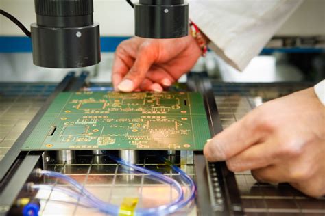
Inspection and Testing: After fabrication, the PCBs undergo rigorous inspection and testing to ensure they meet the required specifications. This includes visual inspection, electrical testing, and functional testing.
-
Assembly: Finally, the PCB is assembled with the necessary components, such as resistors, capacitors, and integrated circuits. This can be done manually or using automated assembly machines.
PCB Assembly Techniques
PCB assembly is the process of populating a PCB with electronic components. There are several techniques used for PCB assembly, each with its own advantages and disadvantages.
Through-Hole Assembly
Through-hole assembly is the traditional method of PCB assembly, where components with long leads are inserted into holes drilled in the PCB and soldered in place. This technique is well-suited for larger components and provides a strong mechanical connection. However, it is slower and more labor-intensive than surface mount assembly.
Surface Mount Assembly
Surface mount assembly, also known as SMT (Surface Mount Technology), is a more modern technique where components are mounted directly onto the surface of the PCB. This allows for smaller components and higher component density compared to through-hole assembly. SMT is faster and more efficient than through-hole assembly, making it the preferred choice for high-volume production.
Mixed Assembly
Mixed assembly is a combination of through-hole and surface mount assembly techniques. This is often used when a PCB requires both types of components, such as connectors or large capacitors that are not available in surface mount packages.

PCB Assembly Equipment
To perform PCB assembly efficiently and accurately, specialized equipment is used. Some of the key pieces of equipment include:
-
Pick and Place Machine: This automated machine is used to pick up components from reels or trays and place them onto the PCB with high precision. Modern pick and place machines can place thousands of components per hour, making them essential for high-volume production.
-
Reflow Oven: After the components are placed on the PCB, the board is passed through a reflow oven. This heats the solder paste, causing it to melt and form a permanent connection between the components and the PCB.
-
Wave Soldering Machine: For through-hole assembly, a wave soldering machine is used. The PCB is passed over a molten solder wave, which fills the through-holes and creates a solder joint.
-
Inspection Systems: Various inspection systems, such as automated optical inspection (AOI) and X-ray inspection, are used to ensure the quality and accuracy of the assembled PCB.

PCB Manufacturing and Assembly Considerations
When manufacturing and assembling PCBs, several important factors must be considered to ensure the best possible outcome:
Design for Manufacturability (DFM)
DFM is the practice of designing PCBs in a way that optimizes their manufacturability. This involves adhering to design guidelines, such as minimum trace widths and spacing, hole sizes, and component placement. By following DFM principles, designers can minimize manufacturing issues and improve the overall quality of the PCB.
Component Selection
Choosing the right components is crucial for the success of a PCB. Factors to consider include:
– Availability: Ensure that the selected components are readily available and not at risk of becoming obsolete.
– Cost: Consider the cost of the components and how they impact the overall cost of the PCB.
– Performance: Select components that meet the required specifications and performance criteria for the intended application.
Quality Control
Implementing a robust quality control process is essential to ensure the reliability and functionality of the manufactured PCBs. This includes:
– Incoming inspection of materials and components
– In-process inspection during fabrication and assembly
– Final inspection and testing of the assembled PCB
– Traceability and documentation of the manufacturing process
By adhering to strict quality control measures, manufacturers can minimize defects and ensure that the PCBs meet the required standards.

PCB Manufacturing Data and Statistics
The global PCB market is a vast and growing industry. Here are some key statistics and data points:
| Statistic | Value |
|---|---|
| Global PCB Market Size (2020) | $60.2 billion |
| Projected Market Size (2027) | $75.7 billion |
| CAGR (2021-2027) | 3.3% |
| Largest Market Share | Asia Pacific (90%) |
| Top PCB Manufacturing Countries | China, Taiwan, South Korea, Japan, United States |
Source: https://www.grandviewresearch.com/industry-analysis/printed-circuit-board-pcb-market
Frequently Asked Questions (FAQ)
-
What is the difference between a single-layer and multi-layer PCB?
A Single-Layer PCB has conductive traces on only one side of the substrate, while a multi-layer PCB has conductive traces on both sides and/or has additional layers sandwiched between the top and bottom layers. Multi-layer PCBs offer higher component density and better signal integrity compared to single-layer PCBs. -
What is the purpose of a solder mask on a PCB?
A solder mask is a protective coating applied to the copper traces of a PCB. It serves to insulate the traces, prevent short circuits, and protect against oxidation. The solder mask also provides a surface for the application of component labels and other markings. -
What are the advantages of surface mount assembly over through-hole assembly?
Surface mount assembly offers several advantages, including: - Smaller component sizes and higher component density
- Faster assembly speeds and higher throughput
- Lower assembly costs due to automation
-
Improved signal integrity due to shorter lead lengths
-
What is the role of a pick and place machine in PCB assembly?
A pick and place machine is an automated system that picks up electronic components from reels or trays and places them onto the PCB with high precision. This machine is essential for high-volume PCB assembly, as it can place thousands of components per hour, significantly reducing assembly time and costs compared to manual placement. -
Why is design for manufacturability (DFM) important in PCB manufacturing?
DFM is important because it ensures that the PCB Design is optimized for the manufacturing process. By adhering to DFM guidelines, designers can minimize manufacturing issues, such as poor solderability, insufficient clearances, or difficulty in component placement. This leads to higher yields, lower costs, and improved overall quality of the manufactured PCB.
Conclusion
PCB manufacturing and assembly are critical processes in the production of modern electronic devices. By understanding the various steps involved in PCB manufacturing, the different assembly techniques, and the key considerations for ensuring quality and reliability, designers and manufacturers can work together to create high-performance PCBs that meet the demands of today’s applications.
As the electronics industry continues to evolve, so too will the technologies and processes used in PCB manufacturing and assembly. By staying up-to-date with the latest developments and best practices, manufacturers can remain competitive and deliver the best possible products to their customers.
No responses yet