Introduction to PCB Manufacturing
Printed Circuit Board (PCB) manufacturing is a complex process that involves multiple steps and considerations. To ensure the production of high-quality PCBs, it is essential to understand and adhere to the recommended points throughout the manufacturing process. This article will provide a comprehensive overview of the key aspects to keep in mind during PCB manufacturing.
Understanding the PCB Manufacturing Process
Step 1: Design and Layout
The first step in PCB manufacturing is the design and layout of the circuit board. This involves creating a schematic diagram and a layout file using specialized software such as Altium Designer, Eagle, or KiCad. Some essential points to consider during the design and layout phase include:
- Component placement and orientation
- Trace width and spacing
- Via size and placement
- Power and ground plane design
- Signal integrity and electromagnetic compatibility (EMC)
Step 2: Fabrication
Once the design and layout are finalized, the next step is to fabricate the PCB. This process involves several sub-steps, including:
-
Substrate preparation: The PCB substrate, typically made of FR-4 material, is cut to the required size and cleaned to remove any contaminants.
-
Copper cladding: A thin layer of copper is laminated onto the substrate using heat and pressure.
-
Drilling: Holes are drilled into the PCB for component placement and vias.
-
Plating: The drilled holes are plated with copper to establish electrical connections between layers.
-
Etching: Unwanted copper is removed from the PCB using a chemical etching process, leaving behind the desired traces and pads.
-
Solder mask application: A protective layer called solder mask is applied to the PCB to prevent short circuits and improve the board’s durability.
-
Silkscreen printing: Text, logos, and component identifiers are printed onto the PCB using silkscreen printing.
Step 3: Assembly
After the PCB is fabricated, the components are assembled onto the board. This process can be done manually or using automated equipment, such as pick-and-place machines. The assembly process involves:
-
Solder paste application: Solder paste is applied to the PCB pads using a stencil or syringe.
-
Component placement: Components are placed onto the PCB, either manually or using automated equipment.
-
Reflow soldering: The PCB is heated in a reflow oven, melting the solder paste and creating a permanent connection between the components and the board.
-
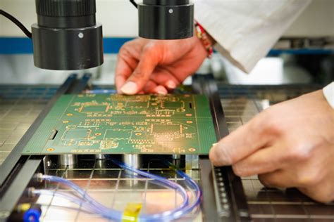
Inspection: The assembled PCB is inspected for any defects or missing components using automated optical inspection (AOI) or manual visual inspection.
Step 4: Testing and Quality Control
The final step in PCB manufacturing is testing and quality control. This ensures that the PCB functions as intended and meets the required specifications. Testing can include:
- In-circuit testing (ICT)
- Functional testing
- Boundary scan testing
- Burn-in testing
Quality control measures, such as visual inspection and X-ray inspection, are also performed to identify any manufacturing defects.

Considerations for High-Quality PCB Manufacturing
To ensure the production of high-quality PCBs, several key factors must be considered throughout the manufacturing process.
Material Selection
Choosing the right materials for your PCB is crucial for its performance and reliability. The most common PCB substrate material is FR-4, which offers good electrical and mechanical properties at a reasonable cost. However, for high-frequency or high-temperature applications, other materials such as Rogers, Teflon, or ceramic may be more suitable.
When selecting materials, consider the following:
- Dielectric constant and loss tangent
- Thermal conductivity and expansion coefficient
- Moisture absorption and environmental stability
- Cost and availability
Design for Manufacturability (DFM)
Designing your PCB with manufacturability in mind can help reduce production costs, improve yield, and minimize defects. Some essential DFM guidelines include:
- Adhering to the manufacturer’s design rules and constraints
- Using standard component sizes and packages
- Avoiding sharp corners and acute angles in trace routing
- Providing adequate spacing between components and traces
- Incorporating testability features, such as test points and boundary scan
Controlled Impedance
For high-speed digital circuits or RF applications, controlling the impedance of the PCB traces is essential to maintain signal integrity and minimize reflections. Controlled impedance is achieved by carefully designing the trace width, thickness, and spacing, as well as the PCB stackup and dielectric properties.
To ensure controlled impedance, consider the following:
- Specifying the target impedance and tolerance
- Providing accurate dielectric material properties to the manufacturer
- Performing impedance testing and validation during production
Thermal Management
Proper thermal management is crucial for the reliability and longevity of your PCB. Overheating can lead to component failure, reduced performance, and even fire hazards. To manage heat dissipation effectively, consider:
- Using thermal vias and planes to conduct heat away from components
- Incorporating heatsinks or fans for high-power components
- Designing adequate spacing and airflow channels between components
- Using thermal interface materials (TIMs) to improve heat transfer
Electromagnetic Compatibility (EMC)
Ensuring electromagnetic compatibility is essential to prevent interference between electronic devices and comply with regulatory requirements. To minimize EMC issues, consider:
- Proper grounding and shielding techniques
- Filtering and suppression of unwanted signals
- Minimizing loop areas and current return paths
- Separating sensitive circuits from noisy ones
Testing and Inspection
Thorough testing and inspection throughout the manufacturing process can help identify and correct defects early, reducing costs and improving quality. Some recommended testing and inspection methods include:
- Automated optical inspection (AOI)
- X-ray inspection
- In-circuit testing (ICT)
- Functional testing
- Boundary scan testing
By incorporating these methods into your manufacturing process, you can catch defects early and ensure that your PCBs meet the required specifications.

Common PCB Manufacturing Defects and How to Prevent Them
Despite the best efforts, PCB manufacturing defects can still occur. Some common defects include:
Solder Bridges
Solder bridges are unintended connections between two or more pads or traces caused by excess solder. To prevent solder bridges:
- Use solder masks to prevent solder from flowing between pads
- Ensure proper solder paste volume and placement
- Optimize reflow soldering parameters
Tombstoning
Tombstoning occurs when a surface-mount component stands up on one end due to uneven heating or solder wetting. To prevent tombstoning:
- Ensure even heating during reflow soldering
- Use symmetrical pad designs and component placement
- Optimize solder paste volume and composition
Lifted Pads
Lifted pads occur when the copper pad separates from the PCB substrate due to mechanical stress or poor adhesion. To prevent lifted pads:
- Ensure proper adhesion between the copper and the substrate
- Avoid excessive mechanical stress during assembly and handling
- Use appropriate pad sizes and shapes
Drill Breakout
Drill breakout occurs when the drill bit exits the PCB at an angle, causing the hole to be misaligned or oversized. To prevent drill breakout:
- Use sharp and well-maintained drill bits
- Optimize drilling parameters, such as feed rate and spindle speed
- Use backup materials to support the PCB during drilling

Best Practices for PCB Manufacturing
To optimize your PCB manufacturing process and ensure the best possible results, consider the following best practices:
Communication and Documentation
Clear communication and comprehensive documentation are essential for successful PCB manufacturing. Provide your manufacturer with:
- Detailed specifications and requirements
- Gerber files and drill files
- Bill of materials (BOM) and assembly drawings
- Any special instructions or considerations
Supplier Selection and Management
Choosing the right PCB manufacturer is crucial for ensuring quality and reliability. When selecting a supplier, consider:
- Their experience and expertise in your specific application
- Their manufacturing capabilities and capacity
- Their quality control and testing procedures
- Their customer support and communication
Establish a strong relationship with your supplier and regularly review their performance to ensure consistent quality and service.
Continuous Improvement
Continuously monitor and improve your PCB manufacturing process to reduce defects, increase efficiency, and lower costs. Some strategies for continuous improvement include:
- Collecting and analyzing production data to identify trends and issues
- Implementing statistical process control (SPC) techniques
- Conducting root cause analysis and corrective action for defects
- Regularly reviewing and updating your design and manufacturing processes
By embracing a culture of continuous improvement, you can stay competitive and adapt to the ever-changing demands of the electronics industry.
Frequently Asked Questions (FAQ)
1. What is the difference between surface-mount technology (SMT) and through-hole technology (THT)?
Surface-mount technology (SMT) involves components that are mounted directly onto the surface of the PCB, while through-hole technology (THT) involves components with leads that are inserted into holes drilled in the PCB and soldered on the opposite side. SMT offers advantages such as smaller component sizes, higher component density, and faster assembly, while THT is more suitable for components that require higher mechanical strength or power handling.
2. What is the purpose of a solder mask on a PCB?
A solder mask is a protective layer applied to the copper traces on a PCB to prevent solder from bridging between pads or traces during the soldering process. It also provides insulation and protection against oxidation and environmental factors, improving the PCB’s durability and reliability.
3. What is the difference between a single-layer and a multi-layer PCB?
A single-layer PCB has conductive traces on only one side of the substrate, while a multi-layer PCB has conductive traces on both sides and/or internal layers. Multi-layer PCBs offer advantages such as higher component density, better signal integrity, and improved EMC performance, but they are more complex and expensive to manufacture compared to single-layer PCBs.
4. What is the purpose of a via in a PCB?
A via is a plated hole that connects conductive traces between different layers of a multi-layer PCB. Vias allow signals and power to be routed vertically through the PCB, enabling more complex and compact designs. There are several types of vias, including through vias, blind vias, and buried vias, each with their own specific applications and manufacturing requirements.
5. What is the difference between a rigid PCB and a flexible PCB?
A rigid PCB is made from a solid, non-flexing substrate material, such as FR-4, while a flexible PCB is made from a thin, flexible substrate material, such as polyimide. Flexible PCBs offer advantages such as the ability to conform to curved or irregular surfaces, reduced weight and space requirements, and improved resistance to vibration and shock. However, they are more complex and expensive to manufacture compared to rigid PCBs.
Conclusion
PCB manufacturing is a complex process that requires careful consideration of numerous factors to ensure the production of high-quality, reliable circuit boards. By understanding the recommended points to note in PCB manufacturing, including material selection, design for manufacturability, controlled impedance, thermal management, EMC, and testing and inspection, you can optimize your manufacturing process and minimize defects.
Additionally, by adopting best practices such as clear communication, supplier management, and continuous improvement, you can stay competitive and adapt to the ever-changing demands of the electronics industry. With the right knowledge and approach, you can successfully navigate the complex world of PCB manufacturing and bring your electronic designs to life.
No responses yet