Introduction to PCB Design
Printed Circuit Board (PCB) design is the process of creating a blueprint for the electrical connections and components that make up an electronic device. It involves the placement of electronic components and the routing of conductive traces on a non-conductive substrate to form a functional circuit. PCB design is a crucial step in the development of electronic products, as it determines the functionality, reliability, and manufacturability of the final product.
Key Aspects of PCB Design
- Schematic Design: Creating a schematic diagram that represents the electrical connections between components.
- Component Selection: Choosing the appropriate electronic components based on the circuit requirements and design constraints.
- Board Layout: Arranging the components and routing the conductive traces on the PCB substrate.
- Design Rule Check (DRC): Verifying that the PCB layout adheres to the manufacturing and electrical constraints.
- Gerber File Generation: Creating the final production files for PCB fabrication.
PCB Design Workflow
Step 1: Schematic Design
The first step in PCB design is creating a schematic diagram that represents the electrical connections between components. The schematic is a symbolic representation of the circuit, using standardized symbols for components and lines for connections. It serves as a blueprint for the PCB layout and helps in understanding the circuit functionality.
Step 2: Component Selection
Once the schematic is complete, the next step is to select the appropriate electronic components for the circuit. This involves considering factors such as:
- Electrical specifications (e.g., voltage rating, current rating, power dissipation)
- Package type and size
- Availability and cost
- Thermal characteristics
- Reliability and quality
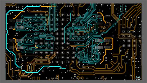
Step 3: Board Layout
The board layout is the process of arranging the components and routing the conductive traces on the PCB substrate. This step is critical for ensuring proper functionality, signal integrity, and manufacturability of the PCB. Key considerations during board layout include:
- Component placement: Arranging components for optimal signal routing and thermal management.
- Trace routing: Creating conductive paths between components while minimizing signal interference and ensuring proper impedance control.
- Layer stackup: Determining the number and arrangement of conductive layers in the PCB.
- Via placement: Adding conductive holes to connect traces between layers.
- Power and ground planes: Designing dedicated layers for power distribution and ground reference.
Step 4: Design Rule Check (DRC)
After completing the board layout, it is essential to perform a Design Rule Check (DRC) to verify that the PCB layout adheres to the manufacturing and electrical constraints. DRC ensures that the design is manufacturable and meets the required specifications. Some common design rules include:
- Minimum trace width and spacing
- Minimum drill size and pad size
- Clearance between components and traces
- Copper pour and thermal relief requirements
Step 5: Gerber File Generation
The final step in PCB design is generating the Gerber files, which are the industry-standard format for PCB fabrication. Gerber files contain the information needed to manufacture the PCB, including the copper layers, solder mask, silkscreen, and drill data. These files are sent to the PCB manufacturer for fabrication.

PCB Layout Techniques
Signal Integrity
Signal integrity is a critical aspect of PCB layout, particularly for high-speed and high-frequency designs. It involves ensuring that signals propagate through the PCB with minimal distortion, reflections, and crosstalk. Some techniques for maintaining signal integrity include:
- Impedance control: Designing traces with consistent impedance to minimize reflections and signal distortion.
- Differential pairs: Routing differential signals together to cancel out electromagnetic interference (EMI).
- Ground planes: Using continuous ground planes to provide a low-impedance return path for signals.
- Decoupling capacitors: Placing decoupling capacitors close to ICs to minimize power supply noise.
Electromagnetic Compatibility (EMC)
Electromagnetic Compatibility (EMC) refers to the ability of electronic devices to operate without causing or being affected by electromagnetic interference. PCB layout plays a crucial role in achieving EMC compliance. Some EMC considerations in PCB layout include:
- Segregating analog and digital circuits: Separating sensitive analog circuits from noisy digital circuits to minimize interference.
- Shielding: Using conductive shields around sensitive components or areas to reduce EMI.
- Grounding: Implementing proper grounding techniques to minimize ground loops and provide a low-impedance path for EMI currents.
- Filtering: Incorporating filters to suppress unwanted high-frequency noise.
Thermal Management
Thermal management is essential for ensuring the reliability and longevity of electronic components. PCB layout can significantly impact the thermal performance of the circuit. Some thermal management techniques in PCB layout include:
- Component placement: Arranging components to minimize thermal coupling and allow for adequate heat dissipation.
- Copper pours: Using large copper areas to spread heat and improve thermal conductivity.
- Thermal vias: Adding vias to transfer heat from components to other layers or heatsinks.
- Heatsinks: Incorporating heatsinks to dissipate heat from high-power components.

PCB Manufacturing
PCB Fabrication Process
The PCB fabrication process involves several steps to convert the PCB design into a physical board. The typical fabrication process includes:
- PCB Printing: Printing the circuit pattern onto a photosensitive film or directly onto the copper-clad laminate.
- Etching: Removing the unwanted copper from the laminate using a chemical etching process.
- Drilling: Drilling holes for through-hole components and vias using CNC machines.
- Plating: Applying a thin layer of copper to the drilled holes to create electrical connections between layers.
- Solder Mask Application: Applying a protective solder mask layer to the PCB to prevent short circuits and improve solderability.
- Silkscreen Printing: Printing text and symbols onto the PCB for component identification and assembly guidance.
- Surface Finish: Applying a surface finish (e.g., HASL, ENIG, OSP) to protect the exposed copper and enhance solderability.
PCB Assembly
After the PCB fabrication process, the board undergoes assembly to populate it with electronic components. The PCB assembly process typically involves:
- Solder Paste Printing: Applying solder paste onto the PCB pads using a stencil or screen printing process.
- Component Placement: Placing the components onto the PCB using automated pick-and-place machines or manual assembly.
- Reflow Soldering: Passing the PCB through a reflow oven to melt the solder paste and form electrical connections between the components and the PCB.
- Inspection and Testing: Performing visual inspection and electrical testing to ensure proper assembly and functionality.

PCB Design Tools
There are various PCB design tools available in the market, ranging from free and open-source software to professional-grade commercial tools. Some popular PCB design tools include:
| Tool | Description |
|---|---|
| Altium Designer | A professional-grade PCB design tool with advanced features |
| KiCad | A free and open-source PCB design tool with a growing community |
| Eagle | A widely used PCB design tool, now owned by Autodesk |
| OrCAD | A comprehensive PCB design solution from Cadence |
| Mentor Graphics PADS | A PCB design tool with strong simulation and analysis capabilities |
Frequently Asked Questions (FAQ)
- What is the difference between a schematic and a PCB layout?
-
A schematic is a symbolic representation of the electrical connections between components, while a PCB layout is the physical arrangement of components and routing of traces on the PCB substrate.
-
What are the common PCB layer stackups?
-
Common PCB layer stackups include single-layer, double-layer, four-layer, and multilayer boards. The choice of layer stackup depends on the complexity of the circuit, signal integrity requirements, and cost considerations.
-
What is the purpose of a solder mask on a PCB?
-
The solder mask is a protective layer applied to the PCB to prevent short circuits and improve solderability. It covers the copper traces, leaving only the exposed pads for component soldering.
-
What is the difference between through-hole and surface-mount components?
-
Through-hole components have leads that are inserted into drilled holes in the PCB and soldered on the opposite side. Surface-mount components are mounted directly onto the PCB pads and soldered using a reflow process.
-
What is the role of a Gerber file in PCB manufacturing?
- Gerber files are the industry-standard format for PCB fabrication. They contain the information needed to manufacture the PCB, including the copper layers, solder mask, silkscreen, and drill data. Gerber files are generated from the PCB design software and sent to the PCB manufacturer for fabrication.
Conclusion
PCB design and layout are essential aspects of electronic product development. By understanding the key principles and techniques involved in PCB design, engineers can create reliable, high-performance, and manufacturable electronic devices. From schematic design to component selection, board layout, and manufacturing considerations, each step in the PCB design process contributes to the overall success of the final product.
As technology advances and electronic systems become more complex, the importance of proper PCB design and layout will only continue to grow. By staying updated with the latest design tools, techniques, and industry standards, PCB designers can overcome challenges and create innovative electronic solutions that meet the evolving needs of the market.
No responses yet