What is PCB Manufacturing?
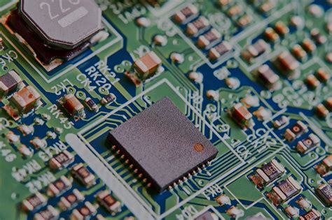
PCB manufacturing is the process of designing and fabricating printed circuit boards (PCBs). A PCB mechanically supports and electrically connects electronic components using conductive tracks, pads and other features etched from one or more sheet layers of copper laminated onto and/or between sheet layers of a non-conductive substrate.
PCBs are used in nearly all electronic products, including computers, smartphones, appliances, medical devices, and of course, Bitcoin miners. The global PCB market size was valued at USD 89.7 billion in 2021 and is expected to expand at a compound annual growth rate (CAGR) of 4.3% from 2022 to 2030.
PCB Manufacturing Process
The PCB manufacturing process typically involves the following steps:
-
Design: The first step is to design the PCB using specialized software such as Altium Designer, KiCad, or Eagle. The design includes the layout of the components, the routing of the traces, and the creation of the Gerber Files that will be used to manufacture the board.
-
Printing: The Gerber files are used to print the PCB design onto a photosensitive film. This film is then used to expose the Copper-Clad Laminate to UV light, which hardens the exposed areas.
-
Etching: The unexposed areas of the copper are then removed using a chemical etching process, leaving behind the desired circuit pattern.
-
Drilling: Holes are drilled into the PCB to allow for the insertion of components and the creation of vias (connections between layers).
-
Plating: The holes are then plated with copper to ensure a good electrical connection.
-
Solder Mask: A solder mask is applied to the PCB to protect the copper traces from oxidation and to prevent solder from bridging between traces.
-
Silkscreen: A silkscreen is applied to the PCB to add text and symbols for easy identification of components and other features.
-
Testing: The PCB is tested to ensure that it functions as intended and meets all specifications.
Here’s a table summarizing the PCB manufacturing process:
| Step | Description |
|---|---|
| Design | Create PCB layout and Gerber files using specialized software |
| Printing | Print PCB design onto photosensitive film |
| Etching | Remove unexposed copper using chemical etching process |
| Drilling | Drill holes for component insertion and vias |
| Plating | Plate holes with copper for electrical connection |
| Solder Mask | Apply solder mask to protect copper traces |
| Silkscreen | Apply silkscreen for text and symbols |
| Testing | Test PCB functionality and specifications |

PCB Assembly for Bitcoin Miners
Once the PCB has been manufactured, it needs to be assembled with the various electronic components required for the Bitcoin miner. This process typically involves the following steps:
-
Solder Paste Application: Solder paste is applied to the pads on the PCB where the components will be placed. This is typically done using a stencil and a squeegee.
-
Pick and Place: The components are then picked up and placed onto the PCB using a machine called a Pick-and-Place machine. This machine uses a vacuum nozzle to pick up the components and place them onto the PCB with high precision.
-
Reflow Soldering: The PCB is then placed into a reflow oven, which heats the solder paste and causes it to melt and form a bond between the component leads and the PCB pads.
-
Inspection: The assembled PCB is then inspected to ensure that all components are properly placed and soldered.
-
Testing: The assembled PCB is then tested to ensure that it functions as intended and meets all specifications.
Here’s a table summarizing the PCB assembly process for Bitcoin miners:
| Step | Description |
|---|---|
| Solder Paste Application | Apply solder paste to PCB pads using stencil and squeegee |
| Pick and Place | Place components onto PCB using pick-and-place machine |
| Reflow Soldering | Melt solder paste in reflow oven to bond components to PCB |
| Inspection | Inspect assembled PCB for proper component placement and soldering |
| Testing | Test assembled PCB functionality and specifications |

Challenges in PCB Manufacturing and Assembly for Bitcoin Miners
PCB manufacturing and assembly for Bitcoin miners can be challenging due to several factors, including:
-
High Power Requirements: Bitcoin miners require a lot of power to operate, which means that the PCBs need to be designed to handle high currents and voltages. This can be challenging from a design and manufacturing perspective.
-
Heat Dissipation: Bitcoin miners generate a lot of heat, which needs to be dissipated to prevent damage to the components. This requires careful design of the PCB layout and the use of heat sinks and other cooling solutions.
-
Compact Design: Bitcoin miners are often designed to be as compact as possible to maximize mining efficiency and reduce costs. This requires careful design of the PCB layout to minimize the size of the board while still accommodating all the necessary components.
-
Component Availability: The high demand for Bitcoin miners can lead to shortages of certain components, which can delay production and increase costs.
-
Quality Control: Bitcoin miners need to operate reliably for long periods of time, which means that quality control is critical. Any defects or failures in the PCB or components can lead to downtime and lost revenue.

Best Practices in PCB Manufacturing and Assembly for Bitcoin Miners
To overcome these challenges and ensure the highest quality and reliability of Bitcoin miner PCBs, manufacturers and assemblers should follow these best practices:
-
Use High-Quality Materials: Use high-quality PCB materials, such as FR-4 or aluminum-backed PCBs, to ensure good thermal conductivity and mechanical stability.
-
Optimize PCB Layout: Optimize the PCB layout to minimize the size of the board while still accommodating all the necessary components and ensuring proper heat dissipation.
-
Use Automated Assembly Processes: Use automated assembly processes, such as pick-and-place machines and reflow ovens, to ensure consistent quality and minimize human error.
-
Implement Strict Quality Control: Implement strict quality control measures, such as automated optical inspection (AOI) and X-ray inspection, to identify and correct any defects or failures in the PCB or components.
-
Work with Reliable Suppliers: Work with reliable suppliers who can provide high-quality components and materials in a timely manner.
Future Trends in PCB Manufacturing and Assembly for Bitcoin Miners
As the demand for Bitcoin miners continues to grow, PCB manufacturers and assemblers will need to innovate to keep up with the latest trends and technologies. Some of the future trends in PCB manufacturing and assembly for Bitcoin miners include:
-
Adoption of Advanced Materials: The use of advanced materials, such as high-performance laminates and thermal interface materials, will become more common to improve the thermal and mechanical performance of Bitcoin miner PCBs.
-
Increased Automation: The use of automation and robotics in PCB manufacturing and assembly will continue to increase to improve efficiency, reduce costs, and ensure consistent quality.
-
Miniaturization: The trend towards miniaturization will continue, with smaller and more compact Bitcoin miner designs becoming more common.
-
Customization: As the Bitcoin mining market becomes more competitive, customization of PCBs and components will become more important to optimize performance and reduce costs.
-
Sustainability: There will be a growing focus on sustainability in PCB manufacturing and assembly, with more manufacturers adopting eco-friendly materials and processes to reduce their environmental impact.
FAQ
-
What is a PCB and why is it important for Bitcoin miners?
A: A PCB (printed circuit board) is a board that mechanically supports and electrically connects electronic components using conductive tracks, pads and other features etched from one or more sheet layers of copper laminated onto and/or between sheet layers of a non-conductive substrate. PCBs are important for Bitcoin miners because they provide the electrical and mechanical foundation for the miner’s components, enabling them to function properly and efficiently. -
What are some of the challenges in PCB manufacturing and assembly for Bitcoin miners?
A: Some of the challenges in PCB manufacturing and assembly for Bitcoin miners include high power requirements, heat dissipation, compact design, component availability, and quality control. These challenges require careful design, high-quality materials, and strict quality control measures to overcome. -
What are some of the best practices in PCB manufacturing and assembly for Bitcoin miners?
A: Some of the best practices in PCB manufacturing and assembly for Bitcoin miners include using high-quality materials, optimizing the PCB layout, using automated assembly processes, implementing strict quality control measures, and working with reliable suppliers. -
What are some of the future trends in PCB manufacturing and assembly for Bitcoin miners?
A: Some of the future trends in PCB manufacturing and assembly for Bitcoin miners include the adoption of advanced materials, increased automation, miniaturization, customization, and a growing focus on sustainability. -
How can I ensure the highest quality and reliability of my Bitcoin miner PCBs?
A: To ensure the highest quality and reliability of your Bitcoin miner PCBs, you should work with experienced and reputable PCB manufacturers and assemblers who follow best practices and implement strict quality control measures. You should also use high-quality materials, optimize your PCB layout, and test your miners thoroughly before deployment.
No responses yet