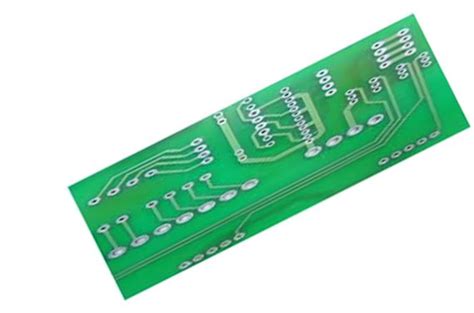
Introduction to Single-Sided PCB
A Single-Sided PCB, also known as a single-layer PCB, is a printed circuit board that has conductive copper traces on only one side of the board. The other side of the board is typically left bare or coated with a solder mask for protection. Single-Sided PCBs are the simplest and most cost-effective type of PCB, making them a popular choice for basic electronic projects and low-complexity circuits.
Advantages of Single-Sided PCBs
- Cost-effective: Single-Sided PCBs are the most affordable type of PCB due to their simple design and manufacturing process.
- Easy to design: With only one layer of conductive traces, Single-Sided PCBs are relatively easy to design compared to multi-layer PCBs.
- Quick turnaround: The manufacturing process for Single-Sided PCBs is faster than that of more complex PCBs, resulting in shorter lead times.
- Suitable for low-complexity circuits: Single-Sided PCBs are ideal for simple electronic projects and low-density circuits.
Disadvantages of Single-Sided PCBs
- Limited routing options: With only one layer of conductive traces, Single-Sided PCBs offer limited routing options, which can make it challenging to design more complex circuits.
- Lower component density: Single-Sided PCBs have a lower component density compared to multi-layer PCBs, as components can only be placed on one side of the board.
- Susceptible to electromagnetic interference (EMI): Single-Sided PCBs are more susceptible to EMI due to the exposed copper traces on one side of the board.
Manufacturing Process of Single-Sided PCBs
The manufacturing process for Single-Sided PCBs involves several steps:
- Substrate preparation: The PCB substrate, typically made of FR-4 (a glass-reinforced epoxy laminate), is cut to the desired size and shape.
- Copper lamination: A thin layer of copper foil is laminated onto one side of the substrate using heat and pressure.
- Drilling: Holes are drilled through the board for component leads and vias (if required).
- Printing: The circuit pattern is printed onto the copper layer using a photoresist material and UV light exposure.
- Etching: The unwanted copper is removed using a chemical etching process, leaving only the desired conductive traces.
- Solder mask application: A solder mask is applied to the board to protect the copper traces and prevent short circuits.
- Silkscreen printing: A silkscreen layer is printed onto the board to add component labels, logos, and other markings.
- Surface finish: A surface finish, such as HASL (Hot Air Solder Leveling) or ENIG (Electroless Nickel Immersion Gold), is applied to the exposed copper to improve solderability and protect against oxidation.

Design Considerations for Single-Sided PCBs
When designing a Single-Sided PCB, there are several factors to consider:
- Component placement: Carefully plan the placement of components to minimize the complexity of the routing and ensure adequate space for traces.
- Trace width and spacing: Ensure that the trace width and spacing meet the manufacturer’s specifications and are appropriate for the current carrying requirements of the circuit.
- Routing: Optimize the routing of traces to minimize the board size and reduce the risk of signal integrity issues.
- Vias: If necessary, use through-hole vias to connect traces on the same side of the board.
- Solder mask and silkscreen: Include a solder mask to protect the copper traces and a silkscreen layer to aid in component placement and identification.

Applications of Single-Sided PCBs
Single-Sided PCBs are used in a variety of applications, including:
- Simple electronic projects: Single-Sided PCBs are ideal for hobbyists and beginners working on basic electronic projects, such as LED circuits or simple sensors.
- Low-complexity devices: Many low-complexity electronic devices, such as remote controls, toys, and basic appliances, use Single-Sided PCBs to keep costs down.
- Prototyping: Single-Sided PCBs are often used for prototyping and testing new designs before moving on to more complex and expensive multi-layer PCBs.
- Educational purposes: Single-Sided PCBs are frequently used in educational settings to teach students about circuit design and PCB manufacturing processes.

Comparison with Other Types of PCBs
Single-Sided PCBs are the simplest and most cost-effective type of PCB, but they have limitations when it comes to circuit complexity and component density. Other types of PCBs offer additional features and benefits:
| PCB Type | Layers | Complexity | Cost | Applications |
|---|---|---|---|---|
| Single-Sided | 1 | Low | Low | Simple projects, prototyping, low-complexity devices |
| Double-Sided | 2 | Medium | Medium | More complex projects, higher component density |
| Multi-Layer | 3+ | High | High | High-speed circuits, dense component placement, advanced electronics |
| Flexible | Varies | Medium to High | High | Wearable electronics, compact devices, applications requiring flexibility |
| Rigid-Flex | Varies | High | Very High | Complex 3D designs, high-reliability applications, aerospace and military |
FAQs
- What is the difference between a Single-Sided PCB and a Double-Sided PCB?
-
A Single-Sided PCB has conductive traces on only one side of the board, while a Double-Sided PCB has traces on both sides, allowing for more complex routing and higher component density.
-
Can Single-Sided PCBs have through-hole components?
-
Yes, Single-Sided PCBs can have through-hole components. The component leads are inserted through drilled holes in the board and soldered to the copper traces on the other side.
-
Are Single-Sided PCBs suitable for high-frequency circuits?
-
Single-Sided PCBs are generally not recommended for high-frequency circuits due to their limited routing options and higher susceptibility to EMI. Multi-layer PCBs are better suited for high-frequency applications.
-
How can I connect traces on a Single-Sided PCB without using vias?
-
To connect traces on a Single-Sided PCB without using vias, you can use Zero-ohm resistors, jumper wires, or component leads to bridge the gaps between traces.
-
What is the typical turnaround time for manufacturing Single-Sided PCBs?
- The turnaround time for manufacturing Single-Sided PCBs is usually faster than that of more complex PCBs. Depending on the manufacturer and the specific requirements of the project, the turnaround time can range from a few days to a couple of weeks.
Conclusion
Single-Sided PCBs are the simplest and most cost-effective type of printed circuit board, making them a popular choice for basic electronic projects, low-complexity devices, and prototyping. While they have limitations in terms of routing options and component density, Single-Sided PCBs offer a quick and affordable solution for many applications.
When designing a Single-Sided PCB, it is essential to consider factors such as component placement, trace width and spacing, and routing optimization. By understanding the manufacturing process and design considerations, you can create successful Single-Sided PCB designs that meet your project’s requirements.
As electronics continue to advance, Single-Sided PCBs will remain an important tool in the designer’s toolkit, providing a foundation for learning and a stepping stone to more complex PCB designs.
No responses yet