What is an HDI PCB?
An HDI PCB is a printed circuit board that features higher wiring density per unit area than conventional PCBs. This is achieved through the use of smaller vias, finer traces, and advanced manufacturing techniques. HDI PCBs allow for the creation of more complex designs in a smaller form factor, making them ideal for applications such as smartphones, tablets, wearables, and medical devices.
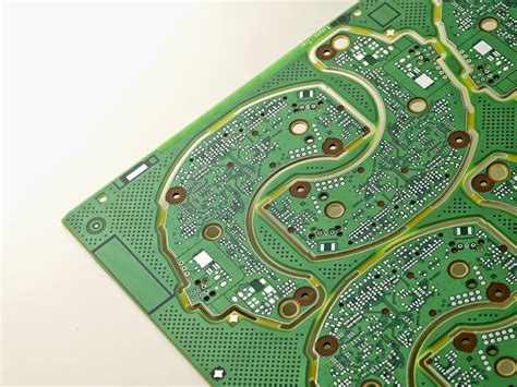
Key Features of HDI PCBs
- High wiring density
- Smaller vias and finer traces
- Thinner substrates
- Blind and buried vias
- Microvias (vias with a diameter less than 150 microns)
Benefits of Using HDI PCBs
1. Miniaturization
One of the primary benefits of HDI PCBs is their ability to enable the miniaturization of electronic devices. By utilizing smaller components and higher wiring density, designers can create more compact and lightweight products without sacrificing functionality.
2. Improved Signal Integrity
HDI PCBs offer improved signal integrity compared to traditional PCBs. The shorter signal paths and reduced cross-talk resulting from the higher wiring density contribute to cleaner and more stable signals, which is crucial for high-speed applications.
3. Enhanced Thermal Management
The compact nature of HDI PCBs allows for better thermal management. The smaller form factor and the use of advanced materials help dissipate heat more efficiently, preventing overheating and ensuring optimal performance.
4. Cost-Effectiveness
Although the initial manufacturing costs of HDI PCBs may be higher than traditional PCBs, they offer long-term cost benefits. The miniaturization and improved functionality enabled by HDI technology can lead to reduced overall system costs, as fewer components and less space are required.

HDI PCB Manufacturing Process
The manufacturing process for HDI PCBs is more complex than that of traditional PCBs due to the higher wiring density and the use of advanced techniques. Here is an overview of the key steps involved:
- Material Selection
- Design and Layout
- Drilling and Via Formation
- Plating and Patterning
- Lamination
- Solder Mask Application
- Surface Finish
- Electrical Testing
- Singulation
1. Material Selection
The choice of substrate material is crucial for HDI PCBs. The most commonly used materials are:
- FR-4: A glass-reinforced epoxy laminate that offers good mechanical and electrical properties.
- Polyimide: A high-performance material with excellent thermal stability and flexibility.
- Rogers: A low-loss, high-frequency material suitable for RF and microwave applications.
2. Design and Layout
The design and layout of HDI PCBs require specialized software and expertise. Designers must adhere to strict design rules to ensure manufacturability and reliability. Key considerations include:
- Via placement and size
- Trace width and spacing
- Impedance control
- Signal integrity
- Thermal management
3. Drilling and Via Formation
HDI PCBs often utilize blind and buried vias, which are drilled using laser or mechanical drilling techniques. Laser drilling is preferred for the creation of microvias, as it offers higher precision and smaller
hole sizes. The formation of blind and buried vias involves multiple drilling and plating steps to create the desired interconnections between layers.
4. Plating and Patterning
After the vias are formed, the PCB undergoes plating and patterning processes. This involves the deposition of copper onto the substrate and into the vias, followed by the selective removal of copper to create the desired circuit patterns. Advanced techniques such as semi-additive processing (SAP) and modified semi-additive processing (mSAP) are often used for HDI PCBs to achieve finer features and higher wiring density.
5. Lamination
For multi-layer HDI PCBs, the individual layers are laminated together under high pressure and temperature. This process ensures a strong bond between the layers and helps maintain the structural integrity of the PCB.
6. Solder Mask Application
A solder mask is applied to the PCB to protect the copper traces from oxidation and to prevent short circuits during the soldering process. The solder mask also provides insulation and improves the aesthetics of the PCB.
7. Surface Finish
The exposed copper pads on the PCB are coated with a surface finish to enhance solderability and protect against corrosion. Common surface finishes for HDI PCBs include:
- Immersion Gold (ENIG)
- Immersion Silver
- Electroless Nickel/Electroless Palladium/Immersion Gold (ENEPIG)
- Organic Solderability Preservative (OSP)
8. Electrical Testing
Rigorous electrical testing is performed to ensure the functionality and reliability of the HDI PCB. This includes:
- Continuity testing
- Insulation resistance testing
- High-voltage testing
- Impedance testing
9. Singulation
Finally, the individual PCBs are cut out from the larger panel using routing or punching techniques. The PCBs are then packaged and shipped to the customer.

Choosing the Right HDI PCB Manufacturing Partner
Selecting the right HDI PCB manufacturing partner is essential for the success of your project. Here are some key factors to consider when making your choice:
1. Experience and Expertise
Look for a manufacturer with a proven track record in HDI PCB fabrication. They should have the necessary technical expertise and experience to handle complex designs and meet your specific requirements.
2. Quality Control
Ensure that the manufacturer has a robust quality control system in place. They should adhere to industry standards such as IPC and ISO, and have a well-documented process for inspecting and testing the PCBs at various stages of production.
3. Capacity and Lead Time
Consider the manufacturer’s production capacity and their ability to meet your required lead times. They should have the necessary equipment and workforce to handle your order volume and deliver the PCBs on schedule.
4. Customer Support
Choose a manufacturer that offers excellent customer support. They should be responsive to your queries, provide timely updates on your project status, and be willing to work closely with you to address any issues that may arise.
5. Cost-Effectiveness
While cost is an important factor, it should not be the sole determining factor when choosing an HDI PCB manufacturer. Strike a balance between cost, quality, and service to ensure the best value for your investment.

Frequently Asked Questions (FAQs)
-
What are the primary applications of HDI PCBs?
HDI PCBs are used in a wide range of applications, including smartphones, tablets, wearables, medical devices, aerospace and defense systems, and automotive electronics. -
How do HDI PCBs differ from traditional PCBs?
HDI PCBs have higher wiring density per unit area compared to traditional PCBs. They feature smaller vias, finer traces, and thinner substrates, enabling the creation of more complex designs in a smaller form factor. -
What are the advantages of using HDI PCBs?
The main advantages of using HDI PCBs are miniaturization, improved signal integrity, enhanced thermal management, and long-term cost-effectiveness. -
What materials are commonly used for HDI PCB substrates?
The most commonly used materials for HDI PCB substrates are FR-4, polyimide, and Rogers. The choice of material depends on the specific requirements of the application, such as thermal stability, electrical performance, and flexibility. -
How can I ensure the quality and reliability of my HDI PCBs?
To ensure the quality and reliability of your HDI PCBs, choose a reputable manufacturer with experience in HDI PCB fabrication. They should have a robust quality control system in place and adhere to industry standards such as IPC and ISO. Additionally, work closely with your manufacturer throughout the design and production process to address any potential issues and optimize your PCB design for manufacturability.
Conclusion
HDI PCBs have become an essential component in the ever-evolving world of electronics. Their ability to enable miniaturization, improve signal integrity, and enhance thermal management has made them indispensable for a wide range of applications. As the demand for smaller, faster, and more powerful devices continues to grow, the importance of HDI PCBs will only increase.
When embarking on an HDI PCB project, it is crucial to choose the right manufacturing partner. Look for a manufacturer with the necessary experience, expertise, and commitment to quality to ensure the success of your project. By working closely with your chosen manufacturer and staying informed about the latest advancements in HDI technology, you can stay ahead of the curve and create innovative, reliable, and cost-effective products.
| Aspect | HDI PCBs | Traditional PCBs |
|---|---|---|
| Wiring Density | High | Low |
| Via Size | Small (microvias) | Larger |
| Trace Width | Fine | Wider |
| Substrate Thickness | Thin | Thicker |
| Via Types | Blind, buried, and through-hole | Primarily through-hole |
| Applications | Smartphones, wearables, medical devices | Larger electronic devices |
| Manufacturing Complexity | High | Lower |
| Cost | Initially higher, but cost-effective in the long run | Lower initial cost |
Table: Comparison between HDI PCBs and Traditional PCBs
In conclusion, HDI PCBs are revolutionizing the electronics industry by enabling the creation of smaller, faster, and more powerful devices. By understanding the benefits, manufacturing process, and key considerations when choosing an HDI PCB manufacturing partner, you can unlock the full potential of this technology and stay at the forefront of innovation in your industry.
No responses yet