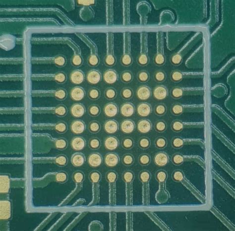
What is a PCB Via?
A Printed Circuit Board (PCB) via is a small hole drilled through a PCB that allows electrical connections to be made between different layers of the board. Vias are essential components in multi-layer PCBs as they enable the routing of signals and power between layers, making more complex designs possible in a compact space.
How PCB Vias Work
PCB vias are created by drilling holes through the board and then plating the inside of the hole with a conductive material, typically copper. This creates an electrical connection between the layers of the PCB that the via passes through.
The size of the via depends on the design requirements and the capabilities of the PCB manufacturer. Smaller vias allow for denser packaging of components but are more difficult and expensive to manufacture.
Types of PCB Vias
There are several types of PCB vias, each with its own characteristics and applications. The main types are:
Through-Hole Vias
Through-hole vias are the most common type of via. They pass completely through the PCB, from the top layer to the bottom layer. They are typically used for mounting through-hole components or for making connections between layers in simpler designs.
| Advantages | Disadvantages |
|---|---|
| Easy to manufacture | Consumes more board space than other via types |
| Provides strong mechanical connection | Limits the density of components on the board |
| Suitable for through-hole component mounting | Higher impedance than other via types |
Blind Vias
Blind vias are vias that start on an outer layer of the PCB and terminate on an inner layer, without going through the entire board. They are used to connect an outer layer to one or more inner layers, but not to the opposite outer layer.
| Advantages | Disadvantages |
|---|---|
| Allows for higher component density | More expensive to manufacture than through-hole vias |
| Reduces the amount of board space used by vias | Requires more complex manufacturing processes |
| Provides more flexibility in signal routing | Limited to connecting outer layers to inner layers |
Buried Vias
Buried vias are vias that connect two or more inner layers of a PCB without extending to either of the outer layers. They are used to make connections between inner layers in more complex designs.
| Advantages | Disadvantages |
|---|---|
| Allows for even higher component density | Most expensive via type to manufacture |
| Frees up space on outer layers for components | Requires advanced manufacturing capabilities |
| Provides the most flexibility in signal routing | Limited to connecting inner layers |
Microvias
Microvias are very small vias, typically with a diameter of 0.15mm or less. They are used in high-density designs to make connections between very closely spaced layers.
| Advantages | Disadvantages |
|---|---|
| Allows for the highest component density | Requires specialized manufacturing equipment |
| Ideal for connecting fine-pitch components | More expensive than larger vias |
| Enables the most compact PCB designs | Can be less reliable than larger vias |

Choosing the Right Type of Via
The choice of via type depends on several factors, including:
- The complexity of the PCB design
- The required component density
- The signal routing requirements
- The manufacturing capabilities of the PCB fabricator
- The budget for the project
For simpler designs with lower component density, through-hole vias are often sufficient and the most cost-effective option. As the complexity and component density of the design increases, blind and buried vias become necessary to make all the required connections while minimizing the board size.
For very high-density designs, such as those used in smartphones or other compact electronics, microvias are essential to achieve the necessary component density and signal routing.
It’s important to work closely with your PCB manufacturer to determine the best via type for your specific design. They can advise you on the capabilities of their manufacturing process and help you find the most cost-effective solution that meets your design requirements.

PCB Via Manufacturing Process
The manufacturing process for PCB vias varies depending on the type of via and the capabilities of the PCB fabricator. However, the basic steps are as follows:
-
Drilling: Holes are drilled through the PCB at the locations where vias are required. The size of the drill bit determines the diameter of the via.
-
Plating: The inside of the drilled holes is plated with a conductive material, typically copper, to create the electrical connection between layers.
-
Filling (optional): For some types of vias, such as blind or buried vias, the holes may be filled with a non-conductive material to improve the structural integrity of the board and to prevent the entrapment of contaminants.
-
Capping (optional): In some cases, the via may be capped with a conductive material on the outer layers to improve the electrical performance and to prevent the via from being exposed to the environment.
The specific manufacturing process used will depend on the type of via and the requirements of the design. More complex via types, such as buried or microvias, require more advanced manufacturing equipment and processes, which can increase the cost and lead time for the PCB.

Design Considerations for PCB Vias
When designing a PCB that includes vias, there are several important considerations to keep in mind:
-
Via size: The size of the via should be as small as possible to minimize the amount of board space used, but large enough to be reliably manufactured and to provide a good electrical connection.
-
Via placement: Vias should be placed in a way that minimizes the impact on signal integrity and that allows for efficient routing of signals between layers.
-
Via impedance: The impedance of the via should be matched to the impedance of the traces to minimize reflections and signal distortion.
-
Via-in-pad: In some cases, it may be necessary to place a via directly in a component pad. This can save board space but requires careful design to ensure reliable soldering and to avoid interfering with the component placement.
-
Via stubs: Via stubs, which are the unused portions of a via that extend beyond the layers being connected, can cause signal reflections and degrade signal integrity. Careful design is required to minimize the impact of via stubs.
-
Thermal management: Vias can be used to conduct heat away from components and to improve the thermal management of the PCB. This is particularly important for high-power components.
By carefully considering these factors and working closely with your PCB manufacturer, you can ensure that your PCB design is optimized for performance, reliability, and manufacturability.
Frequently Asked Questions (FAQ)
- What is the difference between a through-hole via and a blind via?
-
A through-hole via passes completely through the PCB, from the top layer to the bottom layer, while a blind via starts on an outer layer and terminates on an inner layer without going through the entire board.
-
Why are microvias used in high-density PCB designs?
-
Microvias are used in high-density PCB designs because their small size allows for a higher component density and more efficient use of board space. They are particularly useful for connecting fine-pitch components and for routing signals in compact spaces.
-
How does the choice of via type affect the cost of a PCB?
-
The choice of via type can have a significant impact on the cost of a PCB. Through-hole vias are the least expensive, while blind, buried, and microvias require more advanced manufacturing processes and equipment, which increases the cost. The more complex the via structure, the higher the cost of the PCB.
-
Can vias be used for thermal management in a PCB?
-
Yes, vias can be used for thermal management in a PCB. By placing vias near high-power components and connecting them to thermal planes or heatsinks, heat can be conducted away from the components and dissipated more efficiently. This can help to improve the reliability and performance of the PCB.
-
What is via-in-pad design, and when is it used?
- Via-in-pad design is a technique where a via is placed directly in a component pad, rather than adjacent to it. This can save board space and allow for more compact designs, but it requires careful design to ensure reliable soldering and to avoid interfering with the component placement. Via-in-pad design is commonly used in high-density PCBs where space is at a premium.
Conclusion
PCB vias are essential components in modern electronics, enabling the creation of compact, high-performance devices. By understanding the different types of vias and their characteristics, designers can make informed decisions about which via type to use in their PCB designs.
Through-hole vias are the most common and least expensive, but as the complexity and component density of the design increases, blind, buried, and microvias become necessary to achieve the required performance and functionality.
When designing a PCB with vias, it’s important to consider factors such as via size, placement, impedance, via-in-pad design, via stubs, and thermal management. By working closely with your PCB manufacturer and carefully considering these factors, you can ensure that your PCB design is optimized for performance, reliability, and manufacturability.
As electronics continue to become smaller, faster, and more complex, the role of PCB vias in enabling these advances will only become more important. By staying up-to-date with the latest via technologies and design techniques, PCB designers can continue to push the boundaries of what’s possible in electronic design.
No responses yet