Introduction to PCB Traces
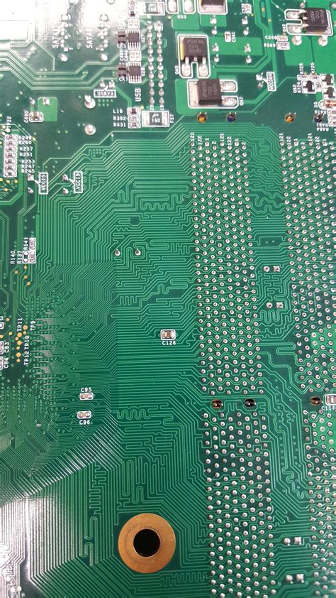
PCB traces are the copper pathways that electrically connect different components on a printed circuit board (PCB). These traces are essential for the proper functioning of the PCB and play a crucial role in determining the overall performance and reliability of the electronic device. In this article, we will dive deep into the world of PCB traces, their importance, design considerations, and best practices.
What are PCB Traces?
PCB traces are thin, conductive paths that are etched or printed onto the surface of a PCB. They are made of copper and are responsible for carrying electrical signals between various components on the board. The width, thickness, and spacing of these traces are critical factors that influence the electrical characteristics of the PCB.
The Role of PCB Traces
PCB traces serve several important functions in the operation of a PCB:
-
Signal Transmission: PCB traces provide a pathway for electrical signals to travel between components on the board. They ensure that signals reach their intended destination with minimal loss and distortion.
-
Power Distribution: Traces also distribute power from the power source to the various components on the PCB. The width and thickness of the traces must be carefully designed to handle the required current without excessive voltage drop or overheating.
-
Grounding: Proper grounding is essential for the stability and noise reduction of a PCB. Ground traces provide a low-impedance path for return currents and help to minimize electromagnetic interference (EMI).
PCB Trace Design Considerations
Designing PCB traces requires careful consideration of several factors to ensure optimal performance and reliability. Let’s explore some of the key design considerations:
Trace Width and Thickness
The width and thickness of PCB traces play a significant role in their electrical characteristics. Wider traces have lower resistance and can carry higher currents, while thicker traces have better mechanical strength and thermal dissipation. However, increasing the width and thickness of traces also increases the overall size of the PCB and can impact the routing density.
The appropriate trace width and thickness depend on several factors, including:
- The required current carrying capacity
- The desired voltage drop
- The available space on the PCB
- The manufacturing capabilities of the PCB fabricator
The following table provides a general guideline for selecting trace width based on the current requirements:
| Current (A) | Trace Width (mm) |
|---|---|
| 0.5 | 0.2 |
| 1.0 | 0.4 |
| 2.0 | 0.8 |
| 3.0 | 1.2 |
| 5.0 | 2.0 |
It’s important to note that these are just guidelines, and the actual trace width should be calculated based on the specific requirements of the design.
Trace Spacing and Clearance
The spacing between PCB traces is another critical design consideration. Adequate spacing is necessary to prevent signal crosstalk, reduce EMI, and ensure proper insulation between traces. The minimum spacing between traces depends on several factors, including:
- The voltage difference between adjacent traces
- The speed and frequency of the signals
- The manufacturing capabilities of the PCB fabricator
The IPC (Association Connecting Electronics Industries) provides guidelines for minimum trace spacing based on the voltage difference between traces. Here’s a table summarizing the IPC-2221 standard:
| Voltage Difference (V) | Minimum Spacing (mm) |
|---|---|
| 0-50 | 0.13 |
| 50-100 | 0.25 |
| 100-150 | 0.40 |
| 150-170 | 0.60 |
| 170-250 | 0.80 |
| 250-300 | 1.00 |
| 300-500 | 1.50 |
In addition to trace spacing, it’s important to maintain sufficient clearance between traces and other components, such as vias, pads, and the board edge. The clearance requirements depend on the manufacturing capabilities and the desired level of reliability.
Trace Routing and Topology
The routing and topology of PCB traces also play a crucial role in the performance and reliability of the PCB. Here are some key considerations:
-
Signal Integrity: Proper trace routing is essential for maintaining signal integrity. This involves minimizing signal reflections, crosstalk, and impedance mismatches. Techniques such as controlled impedance routing, differential pair routing, and length matching can help improve signal integrity.
-
EMI Reduction: Careful trace routing can help reduce EMI. Strategies include avoiding long parallel runs of high-speed traces, using ground planes to provide shielding, and implementing proper grounding techniques.
-
Thermal Management: Trace routing should also consider the thermal aspects of the PCB. High-current traces should be routed away from temperature-sensitive components, and sufficient spacing should be provided for heat dissipation.
-
Manufacturing Feasibility: The trace routing must be compatible with the manufacturing capabilities of the PCB fabricator. This includes considerations such as minimum trace width, spacing, and via size.

Best Practices for PCB Trace Design
To ensure optimal performance and reliability of PCB traces, follow these best practices:
-
Use appropriate trace width and thickness: Select trace width and thickness based on the current requirements and manufacturing capabilities. Use online calculators or consult with the PCB fabricator for guidance.
-
Maintain adequate trace spacing: Follow the IPC guidelines for minimum trace spacing based on the voltage difference between adjacent traces. Provide sufficient clearance between traces and other components.
-
Implement proper grounding: Use ground planes and proper grounding techniques to minimize EMI and ensure signal integrity. Provide low-impedance paths for return currents.
-
Consider signal integrity: Use controlled impedance routing, differential pair routing, and length matching for high-speed signals. Minimize signal reflections and crosstalk.
-
Optimize for manufacturability: Design traces that are compatible with the manufacturing capabilities of the PCB fabricator. Avoid overly narrow traces, tight spacing, or complex routing patterns that may increase manufacturing costs or decrease yields.
-
Perform thorough design reviews: Conduct design reviews to catch potential issues early in the design process. Use PCB design tools with built-in design rule checks (DRC) to ensure compliance with manufacturing and electrical requirements.
-
Collaborate with the PCB fabricator: Work closely with the PCB fabricator to ensure that your design is manufacturable and optimized for their processes. Seek their input on trace width, spacing, and other design aspects.

FAQ
-
What is the minimum trace width that can be manufactured?
The minimum trace width depends on the manufacturing capabilities of the PCB fabricator. Typically, trace widths as small as 0.1 mm (4 mil) can be reliably manufactured, but it’s best to consult with your PCB fabricator for their specific capabilities. -
How do I calculate the appropriate trace width for a given current?
The appropriate trace width can be calculated based on the required current carrying capacity, the desired voltage drop, and the PCB material properties. There are online calculators available that can help with this calculation, or you can consult with your PCB fabricator for guidance. -
What is controlled impedance routing?
Controlled impedance routing is a technique used to maintain a constant impedance along a trace to minimize signal reflections and distortions. It involves carefully designing the trace width, thickness, and spacing in relation to the PCB substrate material to achieve the desired impedance. -
How can I reduce EMI in my PCB design?
To reduce EMI in your PCB design, consider the following strategies: - Use proper grounding techniques and ground planes for shielding
- Minimize long parallel runs of high-speed traces
- Use differential pair routing for high-speed signals
- Provide adequate spacing between traces and other components
-
Implement filtering and shielding techniques as necessary
-
What are the benefits of using thicker traces?
Thicker traces offer several benefits: - Increased current carrying capacity
- Lower resistance and voltage drop
- Better mechanical strength and durability
- Improved thermal dissipation
However, thicker traces also increase the overall thickness of the PCB and may impact the routing density.

Conclusion
PCB traces are the lifeblood of any electronic device, enabling the flow of electrical signals and power between components. Proper design and optimization of PCB traces are critical for ensuring the performance, reliability, and manufacturability of the PCB. By considering factors such as trace width, thickness, spacing, routing, and manufacturing capabilities, designers can create PCBs that meet the specific requirements of their applications.
Following best practices and collaborating closely with PCB fabricators can help streamline the design process and minimize potential issues. By paying attention to the details of PCB trace design, designers can create robust and efficient electronic devices that perform reliably in the field.
As technology continues to advance and device complexity increases, the importance of well-designed PCB traces will only continue to grow. By staying up to date with the latest design techniques and manufacturing capabilities, PCB designers can stay ahead of the curve and create innovative electronic solutions that push the boundaries of performance and functionality.
No responses yet