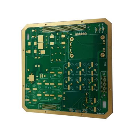
Introduction to Multilayer PCB
A Multilayer PCB, or Printed Circuit Board, is a type of circuit board that consists of multiple layers of conductive material, typically copper, separated by insulating layers. These layers are interconnected using vias, which are small holes drilled through the board and plated with conductive material. Multilayer PCBs offer several advantages over single-layer boards, including increased circuit density, improved signal integrity, and better electromagnetic compatibility (EMC).
Advantages of Multilayer PCBs
- Higher circuit density
- Improved signal integrity
- Better EMC performance
- Reduced size and weight
- Enhanced reliability
Applications of Multilayer PCBs
Multilayer PCBs are widely used in various industries, such as:
- Consumer electronics
- Telecommunications
- Automotive
- Aerospace
- Medical devices
- Industrial automation
Multilayer PCB Construction
PCB Layer Stack-up
A typical multilayer PCB consists of the following layers:
- Top layer (component side)
- Ground plane
- Signal layers
- Power plane
- Bottom layer (solder side)
The number of layers in a multilayer PCB can vary depending on the complexity of the circuit and the application requirements. Common layer counts include 4, 6, 8, 10, 12, and 16 layers.
PCB Material Selection
The choice of PCB material depends on several factors, such as the operating frequency, temperature range, and environmental conditions. Some commonly used PCB materials include:
- FR-4: A glass-reinforced epoxy laminate, suitable for most applications
- Rogers: High-frequency laminates for RF and microwave applications
- Polyimide: High-temperature and flexible PCB materials
- Aluminum: Metal-core PCBs for high-power applications
PCB Thickness and Copper Weight
The thickness of a multilayer PCB is determined by the number of layers and the thickness of each layer. Standard PCB thicknesses range from 0.8 mm to 3.2 mm. The copper weight, or thickness, is typically expressed in ounces per square foot (oz/ft²). Common copper weights include 0.5 oz, 1 oz, and 2 oz.

Multilayer PCB Design Considerations
Signal Integrity
Signal integrity is a critical aspect of multilayer PCB design. Some key considerations include:
- Impedance control: Matching the characteristic impedance of traces to the source and load impedances
- Crosstalk reduction: Minimizing the coupling between adjacent traces
- Reflections: Reducing signal reflections caused by impedance discontinuities
- Transmission line effects: Accounting for the propagation delay and losses in high-speed signals
Power Integrity
Power integrity ensures that the power supply remains stable and free from noise. Some essential factors include:
- Power plane design: Optimizing the power plane layout for low impedance and minimal noise
- Decoupling capacitors: Placing decoupling capacitors close to ICs to reduce power supply noise
- Via placement: Minimizing the inductance of power and ground vias
Thermal Management
Thermal management is crucial for ensuring the reliability and longevity of multilayer PCBs. Some strategies for effective thermal management include:
- Copper pour: Using large copper areas to dissipate heat
- Thermal vias: Placing thermal vias under high-power components to conduct heat to other layers
- Heat sinks: Attaching heat sinks to high-power components for improved heat dissipation
EMC and EMI
Electromagnetic compatibility (EMC) and electromagnetic interference (EMI) are essential considerations in multilayer PCB design. Some techniques for minimizing EMI and ensuring EMC include:
- Shielding: Using shielded enclosures or shielding layers within the PCB
- Grounding: Providing a low-impedance return path for high-frequency currents
- Filtering: Implementing EMI filters to suppress conducted and radiated emissions

Multilayer PCB Manufacturing Process
PCB Fabrication Steps
The manufacturing process for multilayer PCBs involves several steps:
- Inner layer fabrication: Etching the copper patterns on the inner layers
- Lamination: Stacking and bonding the inner layers with insulating prepreg material
- Drilling: Drilling through-holes and vias
- Plating: Electroplating the through-holes and vias with copper
- Outer layer fabrication: Etching the copper patterns on the outer layers
- Solder mask application: Applying a protective solder mask to the outer layers
- Surface finish: Applying a surface finish, such as HASL, ENIG, or OSP
- Silkscreen: Printing component designators and other markings on the PCB
- Electrical testing: Performing continuity and isolation tests to ensure the PCB functions as intended
PCB Assembly Techniques
Once the bare PCB is fabricated, components are assembled onto the board. Two common assembly techniques are:
- Through-hole assembly: Components with leads are inserted into drilled holes and soldered on the opposite side
- Surface-mount assembly: Components are placed directly onto pads on the PCB surface and soldered using reflow or wave soldering processes

Multilayer PCB Testing and Inspection
Electrical Testing
Electrical testing is performed to ensure the PCB functions as intended. Some common electrical tests include:
- Continuity test: Verifying that there are no open circuits or short circuits
- Insulation Resistance (IR) test: Measuring the resistance between isolated conductors
- High-potential (HiPot) test: Applying a high voltage to check for insulation breakdown
Visual Inspection
Visual inspection is conducted to detect any surface defects or assembly issues. Some aspects of visual inspection include:
- Solder joint quality: Checking for proper solder joint formation and the absence of defects like bridging or insufficient solder
- Component placement: Verifying that components are correctly placed and oriented
- Cleanliness: Ensuring the PCB is free from contaminants or debris
Automated Optical Inspection (AOI)
AOI systems use cameras and image processing algorithms to automatically inspect PCBs for defects. AOI can detect issues such as:
- Missing or misaligned components
- Solder defects (bridging, insufficient solder, etc.)
- Incorrect component polarity or orientation
X-ray Inspection
X-ray inspection is used to examine solder joints and other features that are not visible from the surface. X-ray systems can detect:
- Voids or cracks in solder joints
- Proper filling of vias and through-holes
- Correct placement of ball grid array (BGA) components
Multilayer PCB Design Software and Tools
Several software tools are available for designing multilayer PCBs, including:
- Altium Designer
- Cadence OrCAD
- Mentor Graphics PADS
- KiCad
- Eagle
These tools offer features such as schematic capture, PCB layout, 3D modeling, and design rule checking (DRC) to ensure the PCB meets manufacturing and performance requirements.
Frequently Asked Questions (FAQ)
1. What is the difference between a multilayer PCB and a single-layer PCB?
A single-layer PCB has only one conductive layer, while a multilayer PCB has two or more conductive layers separated by insulating layers. Multilayer PCBs offer higher circuit density, improved signal integrity, and better EMC performance compared to single-layer boards.
2. How many layers can a multilayer PCB have?
The number of layers in a multilayer PCB can vary depending on the complexity of the circuit and the application requirements. Common layer counts include 4, 6, 8, 10, 12, and 16 layers, but some high-end applications may require even more layers.
3. What materials are used in multilayer PCB construction?
Common materials used in multilayer PCB construction include FR-4 (a glass-reinforced epoxy laminate), Rogers (high-frequency laminates), polyimide (high-temperature and flexible materials), and aluminum (for metal-core PCBs).
4. What are the key considerations in multilayer PCB design?
Some key considerations in multilayer PCB design include signal integrity (impedance control, crosstalk reduction, reflections, and transmission line effects), power integrity (power plane design, decoupling capacitors, and via placement), thermal management (copper pour, thermal vias, and heat sinks), and EMC/EMI (shielding, grounding, and filtering).
5. What testing and inspection methods are used for multilayer PCBs?
Testing and inspection methods for multilayer PCBs include electrical testing (continuity, insulation resistance, and high-potential tests), visual inspection (solder joint quality, component placement, and cleanliness), automated optical inspection (AOI) for detecting surface defects, and X-ray inspection for examining internal features like solder joints and via filling.
Conclusion
Multilayer PCBs are essential for modern electronic devices, offering high circuit density, improved signal integrity, and better EMC performance. Designing and manufacturing multilayer PCBs involves careful consideration of factors such as layer stack-up, material selection, signal and power integrity, thermal management, and EMC/EMI. A thorough understanding of these aspects, along with the use of appropriate design software and testing methods, is crucial for creating reliable and high-performance multilayer PCBs.
| Layer Count | Typical Application |
|---|---|
| 4 layers | Simple digital circuits, low-speed analog circuits |
| 6 layers | Moderate complexity digital circuits, mixed-signal boards |
| 8 layers | Complex digital circuits, high-speed interfaces |
| 10+ layers | High-density interconnect (HDI) boards, advanced systems |
As electronic devices continue to advance in terms of functionality and performance, the demand for more sophisticated multilayer PCBs will only increase. Staying up-to-date with the latest design techniques, materials, and manufacturing processes will be essential for engineers and designers working on cutting-edge electronic products.
No responses yet