What is a High-Frequency PCB?
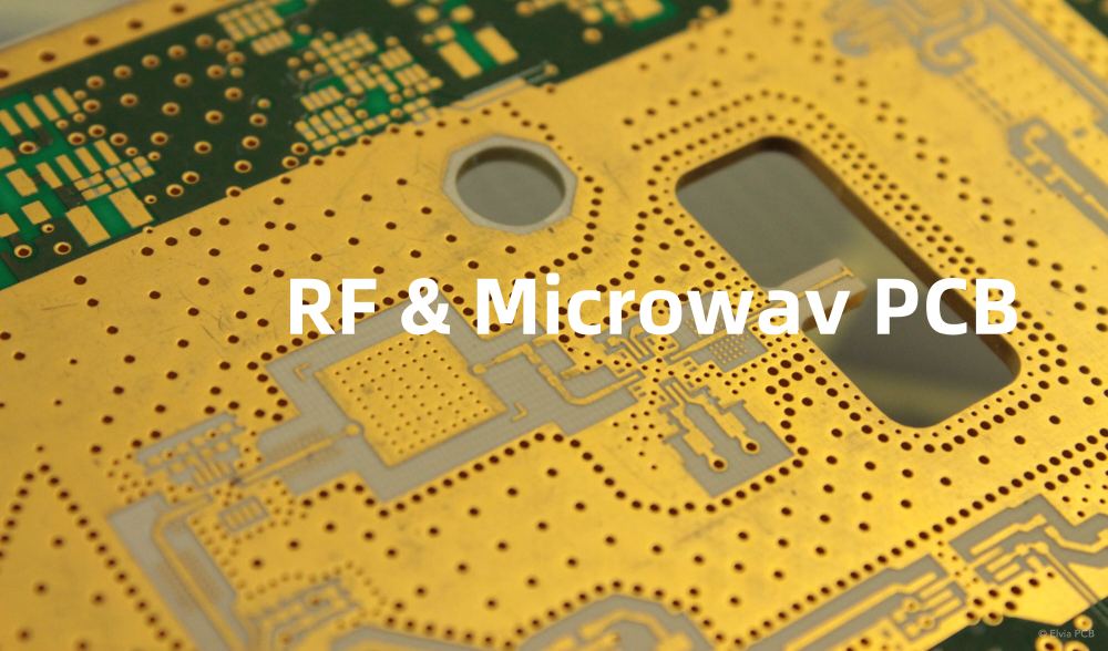
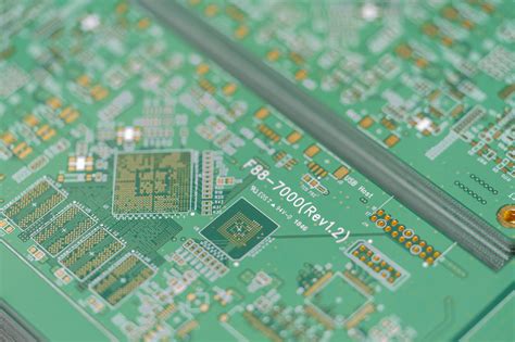
A High-Frequency PCB is a type of printed circuit board that is specifically designed to handle high-speed signals. These PCBs are typically used in applications where signal integrity is critical, such as in telecommunications, aerospace, and defense industries. HF PCBs are characterized by their ability to transmit signals at frequencies above 500 MHz, with some designs capable of handling signals up to 100 GHz or more.
Key Features of High-Frequency PCBs
To achieve high-speed signal transmission, HF PCBs incorporate several key features that distinguish them from traditional PCBs:
-
Low Dielectric Constant (Dk) Materials: HF PCBs use substrate materials with low Dk values, such as polytetrafluoroethylene (PTFE) or hydrocarbon ceramic. These materials minimize signal loss and distortion, allowing for faster signal propagation.
-
Controlled Impedance: HF PCBs are designed with controlled impedance traces to ensure consistent signal integrity. This is achieved by carefully selecting the trace width, thickness, and spacing, as well as the substrate material and thickness.
-
Shielding and Grounding: To reduce electromagnetic interference (EMI) and crosstalk, HF PCBs often incorporate shielding and grounding techniques. This can include the use of ground planes, via stitching, and shielded traces.
-
High-Quality Connectors: HF PCBs require high-quality connectors that can handle high-speed signals without introducing significant loss or distortion. These connectors often feature gold-plated contacts and tight tolerances to ensure reliable performance.
Designing High-Frequency PCBs
Designing an HF PCB requires careful consideration of several factors to ensure optimal signal integrity and performance. Some key design considerations include:
Material Selection
Choosing the right substrate material is critical for HF PCB design. The material must have a low Dk value to minimize signal loss and distortion, as well as good thermal and mechanical properties to ensure reliability. Common substrate materials for HF PCBs include:
| Material | Dielectric Constant (Dk) | Dissipation Factor (Df) | Thermal Conductivity (W/mK) |
|---|---|---|---|
| PTFE (Teflon) | 2.1 | 0.0002 | 0.25 |
| Rogers RO4350B | 3.48 | 0.0037 | 0.62 |
| Isola I-Tera MT40 | 3.45 | 0.0031 | 0.62 |
| Taconic RF-35 | 3.5 | 0.0018 | 0.62 |
Trace Geometry
The geometry of the traces on an HF PCB plays a significant role in signal integrity. To minimize signal reflections and distortions, traces must be designed with controlled impedance. This involves carefully selecting the trace width, thickness, and spacing based on the desired characteristic impedance (typically 50Ω or 75Ω).
| Impedance | Trace Width (mm) | Trace Thickness (mm) | Substrate Thickness (mm) |
|---|---|---|---|
| 50Ω | 0.25 | 0.035 | 0.508 |
| 75Ω | 0.15 | 0.035 | 0.508 |
Via Design
Vias are used to connect traces on different layers of an HF PCB. However, vias can also introduce signal reflections and distortions if not designed properly. To minimize these effects, HF PCBs often use blind and buried vias, which do not extend through the entire thickness of the board. Additionally, via stubs should be minimized or eliminated to reduce signal reflections.
Grounding and Shielding
Proper grounding and shielding are essential for minimizing EMI and crosstalk in HF PCBs. This can be achieved through the use of ground planes, via stitching, and shielded traces. Ground planes provide a low-impedance path for return currents, while via stitching helps to minimize ground bounce and EMI. Shielded traces, such as coplanar waveguides or striplines, can also be used to isolate high-speed signals from other traces on the board.
Manufacturing High-Frequency PCBs
Manufacturing HF PCBs requires specialized equipment and processes to ensure high-quality results. Some key considerations for HF PCB manufacturing include:
Material Handling
HF PCB substrate materials, such as PTFE, can be challenging to work with due to their low surface energy and high coefficient of thermal expansion. Special handling and processing techniques, such as plasma treatment or chemical etching, may be required to ensure proper adhesion and dimensional stability.
Drilling and Plating
Drilling and plating vias in HF PCBs requires high precision and tight tolerances to minimize signal reflections and distortions. Advanced drilling techniques, such as laser drilling or controlled-depth drilling, may be used to create blind and buried vias with minimal stub length. Electroless copper plating is often used to ensure uniform coverage and adhesion of the plating material.
Soldermask and Silkscreen
Applying soldermask and silkscreen to HF PCBs requires careful consideration of the materials and processes used. The soldermask material must have good adhesion and durability, while also providing adequate insulation and protection for the traces. The silkscreen material must be compatible with the soldermask and substrate, and must not introduce significant signal loss or distortion.

Testing and Validation
To ensure that an HF PCB meets the required performance specifications, thorough testing and validation is essential. Some common testing methods for HF PCBs include:
Time-Domain Reflectometry (TDR)
TDR is used to measure the impedance and signal integrity of traces on an HF PCB. By sending a fast-rising pulse down a trace and measuring the reflections, TDR can identify impedance mismatches, discontinuities, and other signal integrity issues.
Vector Network Analysis (VNA)
VNA is used to measure the scattering parameters (S-parameters) of an HF PCB, which describe the signal transmission and reflection characteristics of the board. By measuring the S-parameters over a wide frequency range, VNA can provide a detailed picture of the board’s performance and identify any potential issues.
Eye Diagram Analysis
Eye diagram analysis is used to visualize the quality of a high-speed digital signal on an HF PCB. By overlaying multiple waveforms on top of each other, an eye diagram can reveal signal jitter, noise, and other impairments that can affect signal integrity.
Applications of High-Frequency PCBs
HF PCBs are used in a wide range of applications where high-speed signal transmission is critical. Some common applications include:
Telecommunications
HF PCBs are widely used in telecommunications equipment, such as routers, switches, and base stations. These boards must be able to handle high-speed data transmission over long distances, while also providing reliable performance in harsh environments.
Aerospace and Defense
HF PCBs are also used in aerospace and defense applications, such as radar systems, satellite communications, and electronic warfare. These boards must be able to withstand extreme temperatures, vibrations, and other environmental stresses, while also providing high-speed signal transmission and processing.
Medical Imaging
HF PCBs are used in medical imaging equipment, such as MRI machines and CT scanners. These boards must be able to handle high-speed data acquisition and processing, while also providing high image quality and resolution.
Automotive Electronics
HF PCBs are increasingly being used in automotive electronics, such as advanced driver assistance systems (ADAS) and in-vehicle infotainment systems. These boards must be able to handle high-speed data transmission and processing, while also providing reliable performance in harsh automotive environments.
Frequently Asked Questions (FAQ)
-
What is the difference between a high-frequency PCB and a regular PCB?
A high-frequency PCB is specifically designed to handle signals at frequencies above 500 MHz, while a regular PCB is designed for lower frequency applications. HF PCBs use special materials, geometries, and manufacturing processes to minimize signal loss and distortion at high frequencies. -
What materials are commonly used for high-frequency PCBs?
Common materials for high-frequency PCBs include PTFE (Teflon), Rogers RO4350B, Isola I-Tera MT40, and Taconic RF-35. These materials have low dielectric constants and dissipation factors, which help to minimize signal loss and distortion at high frequencies. -
Why is controlled impedance important for high-frequency PCBs?
Controlled impedance is important for high-frequency PCBs because it helps to minimize signal reflections and distortions. By carefully selecting the trace width, thickness, and spacing based on the desired characteristic impedance, designers can ensure that signals propagate smoothly and with minimal loss. -
What is the purpose of ground planes and via stitching in high-frequency PCBs?
Ground planes and via stitching are used in high-frequency PCBs to minimize electromagnetic interference (EMI) and crosstalk. Ground planes provide a low-impedance path for return currents, while via stitching helps to minimize ground bounce and EMI. -
What are some common testing methods for high-frequency PCBs?
Common testing methods for high-frequency PCBs include time-domain reflectometry (TDR), vector network analysis (VNA), and eye diagram analysis. These methods can help to identify signal integrity issues, measure scattering parameters, and visualize signal quality.

No responses yet