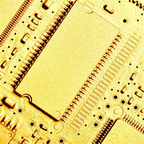
Introduction to Gold PCBs
Gold PCBs, also known as gold-plated printed circuit boards, are a type of PCB that features a thin layer of gold coating on the surface of the copper traces and pads. This gold finishing process is applied to enhance the performance, durability, and reliability of the circuit board in various applications. Gold PCBs are widely used in industries such as aerospace, military, medical devices, and high-end consumer electronics, where superior electrical conductivity, corrosion resistance, and long-term stability are essential.
The Importance of Gold Finishing in PCBs
Gold finishing plays a crucial role in protecting the copper traces and pads on a PCB from oxidation, corrosion, and other environmental factors that can degrade the performance and lifespan of the board. By applying a thin layer of gold, typically ranging from 0.05 to 2.54 microns (2 to 100 microinches), the copper surfaces are shielded from the elements, ensuring reliable electrical connections and preventing signal loss or degradation over time.
Moreover, gold is an excellent conductor of electricity, second only to silver, which makes it an ideal choice for high-frequency and high-speed applications. Gold-plated contact surfaces provide low contact resistance, allowing for efficient signal transmission and minimizing the risk of signal distortion or attenuation.
Methods of Gold Finishing for PCBs
There are two primary methods for applying gold finishing to PCBs: immersion gold (ENIG) and electroplated gold (hard gold). Each method has its advantages and disadvantages, and the choice between them depends on the specific requirements of the application and the budget constraints.
Immersion Gold (ENIG)
Immersion gold, also known as electroless nickel immersion gold (ENIG), is a chemical process that deposits a thin layer of gold onto the copper surfaces of a PCB without the use of electrical current. The process involves several steps:
- Cleaning: The PCB is thoroughly cleaned to remove any contaminants or oxides from the copper surfaces.
- Microetching: A mild etching solution is applied to roughen the copper surfaces, promoting better adhesion of the subsequent layers.
- Nickel plating: A thin layer of nickel (typically 3-6 microns) is deposited onto the copper surfaces through an autocatalytic chemical reaction. The nickel layer serves as a barrier between the copper and the gold, preventing the formation of intermetallic compounds that can weaken the bond.
- Gold plating: The PCB is immersed in a gold solution, where a thin layer of gold (typically 0.05-0.2 microns) is deposited onto the nickel surface through a displacement reaction.
Advantages of immersion gold:
– Cost-effective compared to electroplated gold
– Uniform coverage, even on complex geometries and fine pitch features
– Suitable for surface mount technology (SMT) and wire bonding
– Excellent solderability and wettability
– Good shelf life and storage stability
Disadvantages of immersion gold:
– Thinner gold layer compared to electroplated gold, which may not be suitable for high-wear applications
– Potential for “black pad” formation due to nickel corrosion, especially in high-temperature and high-humidity environments
– Limited rework and repair capabilities
Electroplated Gold (Hard Gold)
Electroplated gold, also known as hard gold or electrolytic gold, is a process that uses an electric current to deposit a thicker layer of gold onto the copper surfaces of a PCB. The process involves the following steps:
- Cleaning: The PCB is cleaned to remove contaminants and oxides from the copper surfaces.
- Activation: The copper surfaces are activated using a mild acid solution to promote better adhesion of the subsequent layers.
- Nickel plating: A layer of nickel (typically 2-5 microns) is electroplated onto the copper surfaces to serve as a barrier and improve the hardness of the gold layer.
- Gold plating: The PCB is immersed in a gold electroplating solution, and an electric current is applied to deposit a thick layer of gold (typically 0.5-2.54 microns) onto the nickel surface.
Advantages of electroplated gold:
– Thicker gold layer provides better wear resistance and durability
– Excellent electrical conductivity and low contact resistance
– Suitable for high-reliability applications, such as connectors and switch contacts
– Better rework and repair capabilities compared to immersion gold
Disadvantages of electroplated gold:
– More expensive than immersion gold due to the thicker gold layer and the use of electrical current
– Potential for uneven coverage on complex geometries and fine pitch features
– Longer processing time compared to immersion gold

Factors to Consider When Choosing Gold Finishing for PCBs
When deciding between immersion gold and electroplated gold for your PCB application, several factors should be taken into account:
-
Application requirements: Consider the specific demands of your application, such as electrical performance, environmental conditions, and mechanical stress.
-
Cost: Evaluate the budget constraints and the cost-benefit ratio of each gold finishing method. Immersion gold is generally more cost-effective, while electroplated gold offers superior performance at a higher price point.
-
Feature size and complexity: Assess the geometry and pitch of the PCB features. Immersion gold is better suited for fine pitch and complex geometries, while electroplated gold may be more appropriate for larger features and simpler designs.
-
Shelf life and storage: Consider the expected shelf life and storage conditions of the PCBs. Immersion gold provides good storage stability, while electroplated gold may be more resistant to oxidation and corrosion over extended periods.
-
Rework and repair: Evaluate the likelihood of rework and repair for your application. Electroplated gold offers better rework capabilities due to its thicker gold layer, while immersion gold may be more challenging to rework without damaging the underlying layers.

Applications of Gold PCBs
Gold PCBs find use in a wide range of industries and applications where high reliability, superior electrical performance, and resistance to harsh environments are critical. Some common applications include:
-
Aerospace and defense: Gold PCBs are used in avionics, satellite communication systems, radar equipment, and military-grade electronics that require high durability and resistance to extreme temperatures, vibrations, and radiation.
-
Medical devices: Gold-plated PCBs are employed in medical diagnostic equipment, implantable devices, and surgical instruments, where biocompatibility, reliability, and long-term stability are essential.
-
Automotive electronics: Gold PCBs are used in high-performance automotive applications, such as engine control units, sensors, and infotainment systems, where they must withstand high temperatures, vibrations, and exposure to harsh chemicals.
-
Telecommunications: Gold-plated PCBs are utilized in high-frequency and high-speed communication systems, such as 5G networks, fiber optic equipment, and satellite transceivers, where signal integrity and low contact resistance are crucial.
-
Consumer electronics: High-end consumer devices, such as smartphones, tablets, and wearables, often incorporate gold PCBs in connectors, switches, and other critical components to ensure reliable performance and long-term durability.

Gold PCB Manufacturing Process
The manufacturing process for gold PCBs involves several key steps to ensure the proper application of the gold finishing and the overall quality of the final product.
-
PCB design and layout: The first step is to design the PCB layout, considering the specific requirements of the application, such as signal integrity, power distribution, and component placement. The design should also take into account the chosen gold finishing method and any associated design rules.
-
PCB fabrication: The PCB is fabricated using standard processes, such as etching, drilling, and plating. The copper traces and pads are formed on the substrate material, and any necessary vias and through-holes are created.
-
Surface preparation: Before applying the gold finishing, the PCB surface must be thoroughly cleaned and prepared to ensure proper adhesion and coverage. This typically involves a combination of cleaning, microetching, and activation steps.
-
Nickel plating: A layer of nickel is plated onto the copper surfaces, either through an electroless process (for immersion gold) or an electrolytic process (for electroplated gold). The nickel layer serves as a barrier between the copper and the gold, improving adhesion and preventing the formation of intermetallic compounds.
-
Gold plating: The gold layer is applied onto the nickel surface, either through an immersion process (for ENIG) or an electroplating process (for hard gold). The thickness and uniformity of the gold layer are carefully controlled to meet the specified requirements.
-
Inspection and testing: After the gold finishing process, the PCBs undergo thorough inspection and testing to ensure compliance with the design specifications and quality standards. This may include visual inspection, electrical testing, and environmental stress testing.
-
Packaging and shipping: The finished gold PCBs are packaged and shipped to the customer, with appropriate handling and storage instructions to maintain the integrity of the gold finishing during transportation and storage.
Quality Control and Testing of Gold PCBs
To ensure the reliability and performance of gold PCBs, strict quality control measures and testing procedures must be implemented throughout the manufacturing process and before final delivery to the customer.
-
Visual inspection: The PCBs are visually inspected for any defects, such as voids, cracks, or contamination in the gold layer, as well as for proper alignment and registration of the features.
-
Thickness measurement: The thickness of the gold layer is measured using non-destructive methods, such as X-ray fluorescence (XRF) or beta backscatter, to ensure compliance with the specified requirements.
-
Adhesion testing: The adhesion of the gold layer to the underlying nickel and copper surfaces is tested using methods such as tape testing or wire pull testing to ensure adequate bonding strength.
-
Solderability testing: The solderability of the gold-plated surfaces is evaluated using wetting balance tests or dip-and-look methods to ensure good wettability and compatibility with the chosen soldering process.
-
Electrical testing: The PCBs undergo electrical testing to verify the continuity, isolation, and impedance of the circuits, as well as to check for any short circuits or open connections.
-
Environmental testing: Depending on the application requirements, gold PCBs may be subjected to various environmental stress tests, such as thermal cycling, humidity exposure, or salt spray testing, to assess their durability and reliability under harsh conditions.
-
Microsectioning: In some cases, destructive testing methods, such as microsectioning, may be employed to examine the cross-section of the PCB and verify the integrity of the gold finishing and the underlying layers.
By implementing comprehensive quality control and testing procedures, manufacturers can ensure that gold PCBs meet the highest standards of reliability and performance, minimizing the risk of defects and failures in the field.
Challenges and Considerations in Gold PCB Manufacturing
While gold PCBs offer numerous benefits in terms of performance and reliability, there are several challenges and considerations that manufacturers must address to ensure the success of their products.
-
Cost: One of the main challenges in gold PCB manufacturing is the relatively high cost of the gold finishing process, especially for electroplated gold, which requires a thicker gold layer and the use of electrical current. Manufacturers must carefully balance the cost of the gold finishing with the performance requirements and budget constraints of the application.
-
Process control: The gold finishing process must be carefully controlled to ensure consistent thickness, uniformity, and adhesion of the gold layer. Factors such as the composition of the plating solutions, the temperature and duration of the plating process, and the surface preparation of the PCB must be closely monitored and optimized.
-
Compatibility with other processes: Gold finishing must be compatible with other manufacturing processes, such as soldering, wire bonding, and component assembly. Manufacturers must consider the specific requirements of these processes and ensure that the gold finishing does not interfere with or degrade the performance of the PCB.
-
Environmental concerns: The use of gold in PCB manufacturing raises environmental concerns, as gold mining and refining can have significant ecological impacts. Manufacturers must strive to minimize waste and implement sustainable practices, such as recycling and recovery of gold from waste streams.
-
Supply chain management: The availability and price of gold can be subject to market fluctuations and geopolitical factors, which can impact the cost and lead time of gold PCBs. Manufacturers must establish robust supply chain management strategies to ensure a stable and reliable source of gold and other raw materials.
-
Skilled workforce: The gold finishing process requires skilled operators and technicians who are knowledgeable about the specific requirements and challenges of the process. Manufacturers must invest in training and development programs to ensure that their workforce has the necessary skills and expertise to produce high-quality gold PCBs.
By addressing these challenges and considerations, manufacturers can optimize their gold PCB production processes, reduce costs, and improve the overall quality and reliability of their products.
Future Trends and Developments in Gold PCB Technology
As the demand for high-performance and reliable electronic devices continues to grow, the gold PCB industry is poised for further advancements and innovations. Some of the key trends and developments that are likely to shape the future of gold PCB technology include:
-
Miniaturization: The ongoing trend towards miniaturization of electronic devices will drive the need for even finer pitch and higher density PCBs. Gold finishing will play a crucial role in enabling reliable interconnections and signal integrity in these highly compact designs.
-
Advanced materials: Researchers are exploring the use of novel materials, such as graphene and carbon nanotubes, in combination with gold finishing to enhance the electrical and thermal properties of PCBs. These advanced materials may enable the development of ultra-high-speed and high-frequency applications.
-
3D printing: The emergence of 3D printing technology for PCB fabrication may open up new possibilities for the application of gold finishing. 3D-printed PCBs with integrated gold-plated features could offer unique design flexibility and customization options.
-
Sustainable manufacturing: As environmental concerns continue to grow, the PCB industry will face increasing pressure to adopt more sustainable manufacturing practices. This may involve the development of eco-friendly gold plating processes, the use of recycled gold, and the implementation of closed-loop recycling systems.
-
Industry 4.0: The integration of advanced technologies, such as artificial intelligence, machine learning, and the Internet of Things (IoT), into the PCB manufacturing process will enable smarter, more efficient, and more responsive production systems. This could lead to improved process control, reduced waste, and higher quality gold PCBs.
-
Collaborative innovation: The future of gold PCB technology will likely be shaped by collaborative innovation among PCB manufacturers, material suppliers, equipment providers, and end-users. By working together to identify and address the evolving needs of the industry, these stakeholders can drive the development of new solutions and best practices for gold PCB manufacturing.
As these trends and developments unfold, the gold PCB industry will continue to play a vital role in enabling the next generation of electronic devices and systems, powering innovation across a wide range of industries and applications.
FAQ
-
What is the difference between immersion gold and electroplated gold?
Immersion gold (ENIG) is a chemical process that deposits a thin layer of gold (typically 0.05-0.2 microns) onto the PCB surface without the use of electrical current. Electroplated gold, also known as hard gold, uses an electric current to deposit a thicker layer of gold (typically 0.5-2.54 microns) onto the PCB surface. Immersion gold is more cost-effective and provides uniform coverage, while electroplated gold offers better wear resistance and durability. -
How does gold finishing protect the copper traces on a PCB?
Gold finishing protects the copper traces on a PCB by creating a barrier layer that prevents oxidation, corrosion, and other environmental factors from degrading the copper surface. The gold layer also provides excellent electrical conductivity and low contact resistance, ensuring reliable signal transmission and minimizing signal loss or distortion. -
What are the main applications for gold PCBs?
Gold PCBs are widely used in industries such as aerospace, military, medical devices, automotive electronics, telecommunications, and high-end consumer electronics. They are particularly well-suited for applications that require high reliability, superior electrical performance, and resistance to harsh environments. -
How can manufacturers ensure the quality and reliability of gold PCBs?
Manufacturers can ensure the quality and reliability of gold PCBs by implementing strict quality control measures and testing procedures throughout the manufacturing process. This includes visual inspection, thickness measurement, adhesion testing, solderability testing, electrical testing, and environmental stress testing. Additionally, manufacturers should follow best practices for process control, materials selection, and supply chain management to minimize defects and ensure consistent performance. -
What are some of the future trends and developments in gold PCB technology?
Some of the key trends and developments in gold PCB technology include miniaturization, the use of advanced materials like graphene and carbon nanotubes, the adoption of 3D printing for PCB fabrication, sustainable manufacturing practices, the integration of Industry 4.0 technologies, and collaborative innovation among industry stakeholders. These trends are expected to drive the development of new solutions and best practices for gold PCB manufacturing, enabling the next generation of high-performance electronic devices and systems.
No responses yet