Introduction to PCB Artwork-Design Guidelines
Printed Circuit Board (PCB) artwork-design is a crucial aspect of PCB manufacturing. It involves creating the layout and design of the copper traces, pads, and other features on the PCB. Proper PCB artwork-design ensures that the manufactured PCB functions as intended, meets the required specifications, and is reliable and durable.
As a PCB manufacturer, it is essential to understand and follow the best practices and guidelines for PCB artwork-design. This article will provide a comprehensive overview of the key PCB artwork-design guidelines that every PCB manufacturer needs to know.
Importance of PCB Artwork-Design Guidelines
Following PCB artwork-design guidelines is crucial for several reasons:
-
Ensuring Functionality: Proper PCB artwork-design ensures that the manufactured PCB functions as intended. It helps in avoiding short circuits, open circuits, and other issues that can affect the performance of the PCB.
-
Meeting Specifications: PCB artwork-design guidelines help in ensuring that the manufactured PCB meets the required specifications, such as the size, thickness, and material properties.
-
Improving Reliability: Following PCB artwork-design guidelines helps in improving the reliability and durability of the manufactured PCB. It minimizes the risk of failures and defects, leading to longer product life and reduced costs.
-
Facilitating Manufacturing: PCB artwork-design guidelines facilitate the manufacturing process by providing clear instructions and standards for the PCB manufacturer to follow. This helps in avoiding errors, delays, and rework during the manufacturing process.

Key PCB Artwork-Design Guidelines
1. Board Size and Shape
The size and shape of the PCB are important considerations in PCB artwork-design. The following guidelines should be followed:
- The board size should be optimized to fit the required components and connectors while minimizing the overall size of the PCB.
- The board shape should be designed to facilitate easy mounting and assembly of the PCB in the final product.
- The board edges should be smooth and free from sharp corners to avoid damage during handling and assembly.
| Board Size | Recommended Dimensions |
|---|---|
| Small | Less than 50mm x 50mm |
| Medium | 50mm x 50mm to 100mm x 100mm |
| Large | Greater than 100mm x 100mm |
2. Component Placement
Proper component placement is crucial for the functionality and reliability of the PCB. The following guidelines should be followed:
- Components should be placed in a logical and organized manner, grouped by function and signal type.
- Sufficient space should be provided between components to allow for proper soldering and assembly.
- Components should be oriented in a consistent direction to facilitate automated assembly processes.
- Critical components, such as high-speed or high-power components, should be placed close to their associated circuitry to minimize signal integrity issues.
3. Trace Routing
Trace routing is the process of creating the copper paths that connect the components on the PCB. The following guidelines should be followed:
- Traces should be routed in a manner that minimizes the length and number of vias.
- Traces should be routed with smooth curves and angles to minimize signal reflections and interference.
- Trace width and spacing should be designed based on the current carrying capacity and the required impedance of the signal.
- High-speed signals should be routed using controlled impedance techniques to maintain signal integrity.
| Trace Width | Current Carrying Capacity |
|---|---|
| 0.2mm | 0.5A |
| 0.3mm | 1A |
| 0.5mm | 2A |
| 1.0mm | 4A |
4. Via Design
Vias are used to connect traces on different layers of the PCB. The following guidelines should be followed for via design:
- Via size and drill diameter should be designed based on the current carrying capacity and the required impedance of the signal.
- Vias should be placed in a manner that minimizes the overall number of vias and the length of the signal path.
- Via-in-pad design should be used for high-density designs to maximize the available routing space.
- Blind and buried vias should be used sparingly to minimize the manufacturing cost and complexity.
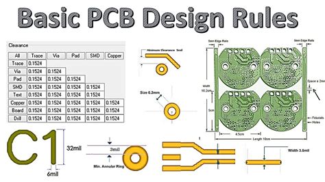
5. Clearance and Creepage
Clearance and creepage are important considerations for ensuring the electrical safety and reliability of the PCB. The following guidelines should be followed:
- Sufficient clearance should be provided between traces and components to prevent short circuits and arcing.
- Creepage distance should be designed based on the voltage and pollution degree of the application.
- Conformal coating or other insulation methods should be used to improve the clearance and creepage performance of the PCB.
| Voltage | Minimum Clearance |
|---|---|
| <50V | 0.1mm |
| 50-100V | 0.2mm |
| 100-150V | 0.3mm |
| >150V | 0.5mm |
6. Solder Mask and Silkscreen
Solder mask and silkscreen are used to protect the PCB and provide visual identification of components and features. The following guidelines should be followed:
- Solder mask should be applied to the PCB to prevent solder bridging and protect the copper traces from oxidation and corrosion.
- Silkscreen should be used to provide clear and legible component identifiers and polarity marks.
- Solder mask and silkscreen should be designed with sufficient clearance from the copper features to prevent bleeding and smearing during the manufacturing process.
7. Panelization
Panelization is the process of combining multiple PCBs into a single panel for manufacturing. The following guidelines should be followed:
- Panelization should be designed to maximize the number of PCBs per panel while minimizing the overall panel size.
- Sufficient space should be provided between the individual PCBs to allow for routing and separation during the depanelization process.
- Fiducial marks and tooling holes should be included in the panel design to facilitate automated assembly and inspection processes.

PCB Artwork-Design Checklist
To ensure that the PCB artwork-design meets the required guidelines, the following checklist should be followed:
- Board size and shape are optimized and meet the required specifications.
- Component placement is logical and organized, with sufficient space for soldering and assembly.
- Trace routing is optimized for signal integrity and manufacturability, with appropriate width and spacing.
- Via design is optimized for current carrying capacity and signal integrity, with minimized via count and length.
- Clearance and creepage are designed based on the voltage and pollution degree of the application, with sufficient spacing and insulation.
- Solder mask and silkscreen are applied with sufficient clearance and legibility.
- Panelization is designed to maximize the number of PCBs per panel and facilitate automated assembly and inspection processes.

Frequently Asked Questions (FAQ)
-
What is the importance of following PCB artwork-design guidelines?
Following PCB artwork-design guidelines is important to ensure the functionality, reliability, and manufacturability of the PCB. It helps in avoiding issues such as short circuits, open circuits, signal integrity problems, and manufacturing defects. -
What are the key considerations for component placement in PCB artwork-design?
The key considerations for component placement include grouping components by function and signal type, providing sufficient space for soldering and assembly, orienting components in a consistent direction, and placing critical components close to their associated circuitry. -
How are trace width and spacing determined in PCB artwork-design?
Trace width and spacing are determined based on the current carrying capacity and the required impedance of the signal. Wider traces are used for higher current carrying capacity, while narrower traces are used for high-speed signals with controlled impedance. -
What is the purpose of solder mask and silkscreen in PCB artwork-design?
Solder mask is used to protect the copper traces from oxidation and corrosion and prevent solder bridging during the soldering process. Silkscreen is used to provide clear and legible component identifiers and polarity marks for assembly and inspection purposes. -
What are the benefits of panelization in PCB artwork-design?
Panelization helps in maximizing the number of PCBs per panel, reducing the overall manufacturing cost and time. It also facilitates automated assembly and inspection processes by providing fiducial marks and tooling holes for alignment and registration.
Conclusion
PCB artwork-design is a critical aspect of PCB manufacturing that requires careful consideration and adherence to best practices and guidelines. By following the guidelines outlined in this article, PCB manufacturers can ensure the functionality, reliability, and manufacturability of their PCBs.
The key guidelines to remember include optimizing the board size and shape, proper component placement, optimized trace routing, appropriate via design, sufficient clearance and creepage, application of solder mask and silkscreen, and effective panelization.
By using the provided checklist and frequently asked questions, PCB manufacturers can verify that their PCB artwork-design meets the required standards and specifications. This will help in avoiding costly errors, delays, and rework during the manufacturing process, ultimately leading to high-quality and reliable PCBs.
No responses yet