What is PCB Assembly?
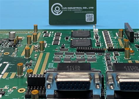
PCB assembly, also known as printed circuit board assembly or PCBA, is the process of soldering or assembly of electronic components onto a printed circuit board (PCB). It is a crucial step in the manufacturing process of electronic devices, as it involves attaching various components such as resistors, capacitors, integrated circuits (ICs), and connectors to the PCB to create a functional electronic assembly.
PCB assembly can be categorized into two main types:
- Through-hole technology (THT) assembly
- Surface mount technology (SMT) assembly
Through-Hole Technology (THT) Assembly
Through-hole technology assembly involves inserting component leads through drilled holes in the PCB and soldering them to pads on the opposite side of the board. This method is generally used for larger components or when higher mechanical stability is required.
Advantages of THT assembly:
– Stronger mechanical bonds between components and the PCB
– Easier to replace or repair components
– Suitable for high-power applications
Disadvantages of THT assembly:
– Slower assembly process compared to SMT
– Requires more space on the PCB
– Higher cost due to manual labor
Surface Mount Technology (SMT) Assembly
Surface mount technology assembly involves placing components directly onto pads on the surface of the PCB and soldering them in place. SMT components are smaller and have shorter leads or no leads at all, allowing for higher component density on the board.
Advantages of SMT Assembly:
– Faster assembly process using automated equipment
– Higher component density, resulting in smaller PCBs
– Lower cost due to reduced manual labor
– Better high-frequency performance
Disadvantages of SMT assembly:
– Requires specialized equipment and skills
– More difficult to replace or repair components
– Not suitable for high-power applications
PCB Assembly Process
The PCB assembly process typically involves the following steps:
- Solder Paste Application
- Component Placement
- Reflow Soldering
- Inspection and Quality Control
- Through-Hole Component Installation (if required)
- Final Assembly and Packaging
1. Solder Paste Application
Solder paste, a mixture of tiny solder spheres and flux, is applied to the PCB pads using a stencil or screen printing process. The stencil ensures that the solder paste is deposited accurately and in the correct amount on each pad.
2. Component Placement
Surface mount components are placed onto the solder paste-covered pads using automated pick-and-place machines. These machines use vacuum nozzles or grippers to pick up components from feeders and place them accurately on the PCB at high speeds.
3. Reflow Soldering
After component placement, the PCB undergoes reflow soldering. The board is passed through a reflow oven, which heats the solder paste to a specific temperature profile, causing the solder to melt and form a permanent connection between the components and the PCB pads.
4. Inspection and Quality Control
After reflow soldering, the PCB undergoes visual and automated optical inspection (AOI) to ensure that all components are correctly placed and soldered. If any defects are found, they are repaired or the board is reworked as necessary.
5. Through-Hole Component Installation (if required)
If the PCB Design includes through-hole components, they are manually inserted and soldered after the SMT process is complete. This step is typically performed using wave soldering or Selective Soldering processes.
6. Final Assembly and Packaging
Finally, the assembled PCB undergoes any additional steps required for the specific application, such as attaching heatsinks, mounting in an enclosure, or adding labels. The completed assembly is then packaged and shipped to the customer.

PCB Assembly Technologies
Several technologies are used in the PCB assembly process to ensure high-quality and efficient production. Some of these technologies include:
Automated Optical Inspection (AOI)
AOI systems use high-resolution cameras and advanced image processing algorithms to inspect assembled PCBs for defects such as missing components, incorrect component placement, and soldering issues. AOI can quickly identify problems and provide feedback for process improvement.
X-Ray Inspection
X-ray inspection is used to examine solder joints and other hidden features that are not visible to the naked eye or AOI systems. This technology is particularly useful for inspecting ball grid array (BGA) and other high-density component packages.
Selective Soldering
Selective soldering is a process that targets specific through-hole components for soldering without exposing the entire board to the soldering process. This method is useful when a PCB contains both SMT and through-hole components, as it allows for localized soldering of the through-hole parts without affecting the SMT components.
Conformal Coating
Conformal coating is a protective layer applied to the assembled PCB to shield it from environmental factors such as moisture, dust, and chemicals. This coating helps to improve the reliability and longevity of the electronic assembly, especially in harsh operating conditions.

Uses and Applications of PCB Assembly
PCB assembly is used in a wide range of industries and applications, including:
- Consumer electronics (smartphones, tablets, laptops, etc.)
- Automotive electronics (engine control units, infotainment systems, etc.)
- Medical devices (patient monitors, imaging equipment, diagnostic tools, etc.)
- Industrial equipment (automation systems, process control, etc.)
- Aerospace and defense (avionics, communication systems, radar, etc.)
- Internet of Things (IoT) devices (smart home appliances, wearables, etc.)
The demand for PCB assembly services continues to grow as electronic devices become increasingly prevalent in our daily lives and across various industries.

Frequently Asked Questions (FAQ)
1. What is the difference between PCB fabrication and PCB assembly?
PCB fabrication is the process of manufacturing the bare printed circuit board, which includes designing the circuit layout, creating the copper traces, and drilling holes. PCB assembly, on the other hand, involves soldering components onto the fabricated PCB to create a functional electronic assembly.
2. What are the most common PCB assembly defects?
Common PCB assembly defects include:
– Solder bridges (unintended connection between two or more solder joints)
– Cold solder joints (insufficient solder or poor solder wetting)
– Tombstoning (one end of a component lifts off the pad during reflow soldering)
– Incorrect component placement or orientation
– Missing components
3. How can I choose the right PCB assembly service provider?
When selecting a PCB assembly service provider, consider the following factors:
– Experience and expertise in your specific industry or application
– Quality certifications (e.g., ISO 9001, IPC standards)
– Production capacity and lead times
– Range of services offered (e.g., prototyping, low-volume, high-volume production)
– Customer support and communication
4. What is the typical turnaround time for PCB assembly?
Turnaround time for PCB assembly varies depending on factors such as the complexity of the design, the number of components, and the production volume. Prototype and low-volume orders may take a few days to a few weeks, while high-volume production runs can take several weeks to months.
5. How can I ensure the quality of my PCB assembly?
To ensure the quality of your PCB assembly, consider the following:
– Work with a reputable PCB assembly service provider with proven quality standards
– Provide clear and accurate design files and documentation
– Communicate your quality requirements and expectations to the service provider
– Request regular quality reports and inspection results throughout the production process
– Perform thorough testing and validation of the assembled PCBs before final acceptance
Conclusion
PCB assembly is a critical process in the production of electronic devices, involving the soldering of components onto a printed circuit board. With the increasing demand for electronic products across various industries, the importance of reliable and efficient PCB assembly services continues to grow. By understanding the different technologies, processes, and best practices involved in PCB assembly, businesses can ensure high-quality and cost-effective production of their electronic assemblies.
No responses yet