Introduction to the 74LS76 Dual JK Flip-Flop
The 74LS76 is a dual JK flip-flop integrated circuit (IC) that belongs to the 74LS family of logic devices. This versatile IC is widely used in digital circuits for various applications such as counters, registers, and control logic. Understanding the 74ls76 pinout is essential for effectively using this IC in your projects.
In this comprehensive guide, we will explore the 74ls76 pinout in detail, including its pin configuration, functions, and applications. We will also discuss how to use the 74LS76 in different circuit designs and provide examples to help you get started.
74LS76 Pin Configuration
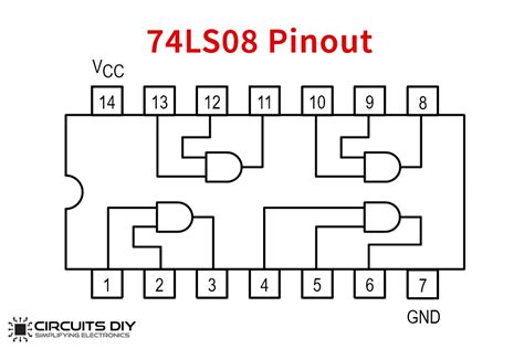
The 74LS76 comes in a 16-pin Dual In-line Package (DIP). The pin configuration of the 74LS76 is as follows:
| Pin Number | Pin Name | Description |
|---|---|---|
| 1 | 1J | J input for flip-flop 1 |
| 2 | 1nQ | Inverted Q output for flip-flop 1 |
| 3 | 1Q | Q output for flip-flop 1 |
| 4 | 1K | K input for flip-flop 1 |
| 5 | 1nCLR | Active-low asynchronous clear input for flip-flop 1 |
| 6 | 1CLK | Clock input for flip-flop 1 |
| 7 | 1nPRE | Active-low asynchronous preset input for flip-flop 1 |
| 8 | GND | Ground |
| 9 | 2nPRE | Active-low asynchronous preset input for flip-flop 2 |
| 10 | 2CLK | Clock input for flip-flop 2 |
| 11 | 2nCLR | Active-low asynchronous clear input for flip-flop 2 |
| 12 | 2K | K input for flip-flop 2 |
| 13 | 2Q | Q output for flip-flop 2 |
| 14 | 2nQ | Inverted Q output for flip-flop 2 |
| 15 | 2J | J input for flip-flop 2 |
| 16 | VCC | Positive supply voltage |
74LS76 Functional Description
The 74LS76 contains two independent JK flip-flops, each with its own set of inputs and outputs. The JK flip-flop is a clocked bistable device that can store one bit of information. The behavior of the flip-flop is determined by the J and K inputs, as well as the clock (CLK) and asynchronous clear (nCLR) and preset (nPRE) inputs.
JK Flip-Flop Truth Table
The truth table for the JK flip-flop is as follows:
| J | K | CLK | nCLR | nPRE | Q(t+1) |
|---|---|---|---|---|---|
| 0 | 0 | ↑ | 1 | 1 | Q(t) |
| 0 | 1 | ↑ | 1 | 1 | 0 |
| 1 | 0 | ↑ | 1 | 1 | 1 |
| 1 | 1 | ↑ | 1 | 1 | nQ(t) |
| X | X | X | 0 | 1 | 0 |
| X | X | X | 1 | 0 | 1 |
Where:
– J and K are the input signals
– CLK is the clock signal (↑ represents a rising edge)
– nCLR is the active-low asynchronous clear signal
– nPRE is the active-low asynchronous preset signal
– Q(t) is the current state of the flip-flop
– Q(t+1) is the next state of the flip-flop
– nQ(t) is the inverted current state of the flip-flop
– X represents a “don’t care” condition
Asynchronous Inputs: nCLR and nPRE
The 74LS76 flip-flops have two asynchronous inputs: nCLR (active-low clear) and nPRE (active-low preset). These inputs allow you to set or reset the flip-flop independently of the clock signal.
- When nCLR is low (0), the flip-flop is reset, and the Q output goes low (0) regardless of the state of the other inputs.
- When nPRE is low (0), the flip-flop is set, and the Q output goes high (1) regardless of the state of the other inputs.
- If both nCLR and nPRE are low simultaneously, the behavior of the flip-flop is undefined.

74LS76 Applications
The 74LS76 dual JK flip-flop finds applications in various digital circuits, such as:
-
Counters: JK flip-flops can be cascaded to create different types of counters, like binary counters, BCD counters, and modulo-N counters.
-
Shift Registers: By connecting multiple flip-flops in series, you can create shift registers for storing and shifting data.
-
Control Logic: JK flip-flops are used in control logic circuits to store and manage the state of the system.
-
Frequency Division: By connecting the inverted output (nQ) of a flip-flop to its J and K inputs, you can create a frequency divider that divides the input clock frequency by 2.
Example Circuit: Modulo-8 Counter
Let’s design a modulo-8 counter using the 74LS76 dual JK flip-flop. A modulo-8 counter counts from 0 to 7 and then resets to 0.
Circuit Diagram
        74LS76          74LS76          74LS76
      +---------+      +---------+      +---------+
      |         |      |         |      |         |
   +--|1J     16|--+   |1J     16|--+   |1J     16|--+
   |  |         |  |   |         |  |   |         |  |
   +--|1nQ     2|  |   |1nQ     2|  |   |1nQ     2|  |
      |         |  |   |         |  |   |         |  |
   +--|1Q      3|--+   |1Q      3|--+   |1Q      3|--+--Output_C
   |  |         |      |         |      |         |
   +--|1K      4|--+   |1K      4|--+   |1K      4|--+
      |         |  |   |         |  |   |         |  |
    --|1nCLR   5|  |   |1nCLR   5|  |   |1nCLR   5|  |
   |  |         |  |   |         |  |   |         |  |
   +--|1CLK    6|--+   |1CLK    6|--+   |1CLK    6|--+--Clock
   |  |         |      |         |      |         |
   +--|1nPRE   7|      |1nPRE   7|      |1nPRE   7|
      |         |      |         |      |         |
      |  GND   8|      |  GND   8|      |  GND   8|
      +---------+      +---------+      +---------+
         |   |            |   |            |   |
         |   +------------+   +------------+   |
         |                                      |
       Output_A                              Output_B
In this circuit, we use three JK flip-flops from two 74LS76 ICs. The J and K inputs of each flip-flop are connected to logic high (1), and the clock inputs are connected to a common clock signal. The nCLR and nPRE inputs are connected to logic high (1) to ensure proper operation.
The outputs of the flip-flops (Q) represent the binary count value, with Output_A being the least significant bit (LSB) and Output_C being the most significant bit (MSB).
Counting Sequence
The modulo-8 counter will follow this counting sequence:
| Count | Output_C | Output_B | Output_A |
|---|---|---|---|
| 0 | 0 | 0 | 0 |
| 1 | 0 | 0 | 1 |
| 2 | 0 | 1 | 0 |
| 3 | 0 | 1 | 1 |
| 4 | 1 | 0 | 0 |
| 5 | 1 | 0 | 1 |
| 6 | 1 | 1 | 0 |
| 7 | 1 | 1 | 1 |
After reaching the count of 7, the counter will reset to 0 on the next clock pulse and repeat the sequence.
Frequently Asked Questions (FAQ)
-
Q: What is the difference between the 74LS76 and 7476?
A: The 74LS76 is a low-power Schottky version of the 7476 dual JK flip-flop. The 74LS76 has a lower power consumption and faster switching speeds compared to the 7476. -
Q: Can the 74LS76 be used as a D flip-flop?
A: Yes, you can use the 74LS76 as a D flip-flop by connecting the J input to the D input and the K input to the inverted D input (nD). When J = D and K = nD, the flip-flop behaves like a D flip-flop. -
Q: How do I create a T flip-flop using the 74LS76?
A: To create a T flip-flop, connect the J and K inputs of the 74LS76 to the T input. This configuration will toggle the flip-flop’s output on each clock pulse when T is high (1). -
Q: What is the maximum clock frequency for the 74LS76?
A: The maximum clock frequency for the 74LS76 depends on the supply voltage and the specific version of the IC. Typically, the maximum clock frequency ranges from 25 MHz to 50 MHz. Consult the manufacturer’s datasheet for the exact specifications. -
Q: Can I replace a 74LS76 with a 74HC76 in my design?
A: Generally, yes. The 74HC76 is a high-speed CMOS version of the 74LS76 and is pin-compatible. However, the 74HC76 has different electrical characteristics, such as higher input impedance and faster switching speeds. Ensure that your design can accommodate these differences before making the substitution.
Conclusion
The 74LS76 dual JK flip-flop is a versatile and widely used IC in digital electronics. By understanding the 74ls76 pinout, its functionality, and its applications, you can effectively use this device in your projects. This guide has provided a comprehensive overview of the 74LS76, including its pin configuration, truth table, and example circuits.
When designing with the 74LS76, consider factors such as power consumption, clock frequency, and the specific requirements of your application. Always consult the manufacturer’s datasheet for detailed specifications and guidelines.
With the knowledge gained from this guide, you can confidently incorporate the 74LS76 into your digital designs and create efficient and reliable circuits.

No responses yet