Introduction to RF PCB Design
RF (radio frequency) PCB (printed circuit board) design is the process of designing circuit boards that can effectively handle high frequency signals for wireless applications. RF PCBs are used in a wide variety of products including cell phones, wireless routers, radars, and satellites. Designing RF PCBs requires specialized knowledge and techniques to ensure signal integrity, minimize noise and interference, and optimize performance.
In this ultimate guide, we will cover everything you need to know about RF PCB design, from the basics of RF theory to advanced design techniques. Whether you are a beginner looking to learn the fundamentals or an experienced designer seeking to refine your skills, this guide has something for you.
RF PCB Design Basics
Before diving into the details of RF PCB design, it’s important to understand some basic concepts and terminology.
What is RF?
RF stands for radio frequency, which refers to the portion of the electromagnetic spectrum with frequencies ranging from about 20 kHz to 300 GHz. RF signals are used for wireless communication and broadcasting applications such as radio, television, cell phones, Wi-Fi, Bluetooth, GPS, and radar.
What is a PCB?
A PCB, or printed circuit board, is a flat board made of insulating material with conductive copper traces printed on one or both sides. PCBs are used to mechanically support and electrically connect electronic components using conductive pathways, tracks, or signal traces etched from copper sheets laminated onto a non-conductive substrate.
RF vs. Digital PCBs
RF PCBs differ from digital PCBs in several key ways:
| RF PCBs | Digital PCBs |
|---|---|
| Handle high frequency analog signals | Handle low frequency digital signals |
| Require careful impedance control | Less sensitive to impedance mismatches |
| Prone to noise and interference | More immune to noise |
| Often use special RF-specific components | Use standard digital components |
| Require specialized layout techniques | Can use general PCB layout techniques |
Key RF PCB Design Considerations
When designing RF PCBs, there are several key considerations to keep in mind:
- Signal integrity – ensuring that the desired signal reaches its destination with minimal distortion, attenuation, or interference
- Impedance control – matching the impedance of the signal path to the source and load to minimize reflections and power loss
- Grounding and shielding – providing low-impedance return paths for currents and shielding sensitive circuits from external noise sources
- Transmission line effects – accounting for the propagation delay, attenuation, and dispersion of signals traveling along PCB traces
- Component selection and placement – choosing RF-specific components and placing them optimally to minimize parasitics and coupling
- Manufacturing constraints – designing the PCB to be compatible with the chosen manufacturing process and materials
By understanding and addressing these key considerations, you can design high-performance RF PCBs that meet your application requirements.

RF PCB Material Selection
Choosing the right PCB material is critical for RF applications, as the material properties directly impact signal propagation, loss, and impedance. The most common RF PCB materials are:
FR-4
FR-4 is a widely used, low-cost PCB material composed of woven fiberglass cloth with an epoxy resin binder. It has reasonable mechanical and electrical properties, but its high loss tangent and variability make it unsuitable for most RF applications above a few hundred MHz.
Rogers
Rogers Corporation offers a range of high-performance PCB materials optimized for RF applications, such as:
- RO4000 series – glass-reinforced hydrocarbon/ceramic laminates with low loss tangent and stable dielectric constant
- RT/duroid – PTFE-based composites with low loss tangent and uniform dielectric constant
- TMM – thermoset ceramic laminates with low loss tangent and high thermal conductivity
These materials offer superior electrical performance compared to FR-4, but at a higher cost.
PTFE
Polytetrafluoroethylene (PTFE) is a synthetic fluoropolymer with excellent electrical and thermal properties. PTFE-based PCB materials, such as Teflon and Taconic TLY, have very low loss tangent and stable dielectric constant, making them ideal for high-frequency RF applications. However, PTFE is more expensive and harder to process than other materials.
Isola
Isola Group offers a range of mid-performance PCB materials that balance cost and performance, such as:
- I-Tera MT – low-loss, high-Tg, low-moisture-absorption material for cost-sensitive RF applications
- Astra MT – low-loss, high-Tg, halogen-free material with improved thermal reliability
These materials provide a good compromise between the low cost of FR-4 and the high performance of Rogers and PTFE materials.
When selecting an RF PCB material, consider the following factors:
- Dielectric constant (Dk) – affects the wavelength and impedance of signals propagating through the material
- Loss tangent (Df) – measures the amount of energy lost as heat in the material
- Thermal coefficient of Dk – indicates how much the Dk changes with temperature
- Moisture absorption – affects the stability of the Dk and can lead to signal degradation
- Cost and availability – higher-performance materials are generally more expensive and may have longer lead times
By choosing the right material for your RF PCB, you can ensure optimal signal integrity and performance while balancing cost and manufacturability constraints.

RF PCB Stackup Design
The PCB stackup refers to the arrangement of conductive and insulating layers in a PCB. Proper stackup design is crucial for RF PCBs, as it affects impedance, crosstalk, and electromagnetic compatibility (EMC). Here are some guidelines for designing RF PCB stackups:
Use Thin Dielectrics
Thin dielectric layers between the signal and ground planes help to reduce the characteristic impedance of the traces, allowing for narrower traces and smaller components. This is particularly important for high-frequency designs, where the wavelength of the signals becomes comparable to the dimensions of the PCB features.
Minimize Layer Count
Fewer layers in the stackup can reduce the overall thickness of the PCB, which is beneficial for RF applications. Thinner PCBs have lower dielectric losses and are easier to manufacture with tight tolerances. However, the layer count should still be sufficient to accommodate all the necessary signal, power, and ground planes.
Use Symmetrical Stackups
A symmetrical stackup, where the layer arrangement is mirrored around the center core, helps to balance the mechanical stresses in the PCB and prevent warping. It also ensures that the characteristic impedance of the traces is consistent on both sides of the board.
Provide Adequate Grounding
Solid ground planes should be placed adjacent to each signal layer to provide a low-impedance return path for the signals. This helps to minimize crosstalk and EMI, and stabilizes the characteristic impedance of the traces. In some cases, a dedicated ground layer may be necessary to ensure proper grounding.
Consider Shielding
For sensitive RF circuits, it may be necessary to include shielding layers in the stackup. These are typically solid copper planes that are grounded at the edges of the board to create a Faraday cage around the sensitive components. Shielding layers can help to reduce external EMI and prevent coupling between different sections of the board.
Here is an example of a 6-layer RF PCB stackup:
| Layer | Material | Thickness (mils) | Function |
|---|---|---|---|
| 1 | Copper | 1.4 | Signal |
| – | RO4350B | 8 | Dielectric |
| 2 | Copper | 1.4 | Ground |
| – | RO4450B | 40 | Core |
| 3 | Copper | 1.4 | Power |
| – | RO4450B | 40 | Core |
| 4 | Copper | 1.4 | Ground |
| – | RO4350B | 8 | Dielectric |
| 5 | Copper | 1.4 | Signal |
This stackup uses Rogers RO4000-series materials for the dielectric layers and a symmetrical arrangement of signal, ground, and power planes. The thin 8-mil dielectric layers help to control the impedance of the traces, while the thicker 40-mil core layers provide mechanical stability.
By following these guidelines and carefully designing your RF PCB stackup, you can ensure optimal signal integrity, EMC, and manufacturability for your RF application.

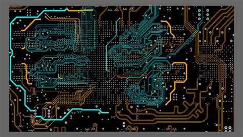
RF PCB Layout Techniques
Once you have selected your RF PCB material and designed your stackup, the next step is to lay out the PCB. RF PCB layout requires special techniques to minimize signal degradation, crosstalk, and EMI. Here are some key RF PCB layout techniques:
Transmission Line Routing
RF signals on PCBs behave as transmission lines, which have characteristic impedance and propagation velocity determined by the trace geometry and dielectric properties. To ensure proper impedance matching and signal integrity, RF traces should be routed as controlled-impedance transmission lines, such as microstrip, stripline, or coplanar waveguide (CPW).
The width and spacing of the traces should be carefully calculated based on the desired characteristic impedance, typically 50 ohms for most RF applications. Online calculators or PCB design software can help with these calculations.
Length Matching
In RF circuits, it is often necessary to match the electrical length of different signal paths to ensure proper phase alignment and timing. This is especially important for differential pairs, where any length mismatch can cause mode conversion and signal degradation.
To match the lengths of RF traces, you can use serpentine routing, meandering, or delay lines. The goal is to make the electrical length of each trace equal, while minimizing any impedance discontinuities or crosstalk.
Grounding and Shielding
Proper grounding and shielding are essential for RF PCBs to minimize noise, crosstalk, and EMI. Here are some techniques to improve grounding and shielding:
- Use solid ground planes instead of gridded or hatched planes to provide a low-impedance return path for currents.
- Avoid splitting ground planes or running signals across split planes, as this can cause impedance mismatches and signal degradation.
- Use via stitching or fencing around sensitive RF circuits to create a Faraday cage and shield them from external EMI.
- Place ground vias near the edges of the board and around connectors to provide a low-impedance path for any external noise to be shunted to ground.
- Use guard traces or co-planar ground traces around sensitive RF traces to minimize crosstalk and provide additional shielding.
Component Placement
The placement of RF components on the PCB can have a significant impact on signal integrity and performance. Here are some guidelines for RF component placement:
- Place RF components as close as possible to their associated traces and vias to minimize parasitic inductance and capacitance.
- Orient RF components to minimize coupling and crosstalk between adjacent components or traces.
- Avoid placing RF components near the edges of the board or near connectors, as these areas are more susceptible to EMI.
- Use symmetry and balance in the placement of differential components, such as baluns or filters, to ensure equal propagation delays and impedances.
- Provide adequate grounding and heat sinking for RF power amplifiers and other high-power components.
Routing Techniques
When routing RF traces on the PCB, there are several techniques to minimize signal degradation and impedance discontinuities:
- Use smooth, gradual bends instead of sharp corners to minimize reflections and radiation.
- Avoid routing RF traces near the edges of the board or near other high-speed traces to minimize crosstalk.
- Use via fencing or stitching to isolate RF traces from other signals and provide additional shielding.
- Avoid using stubs or unterminated traces, as these can cause reflections and resonances that degrade signal quality.
- Use tapered or mitered bends to match the impedance of the traces and minimize discontinuities.
By applying these RF PCB layout techniques, you can ensure that your RF design performs optimally and meets your application requirements.
RF PCB Simulation and Verification
Before sending your RF PCB design for manufacturing, it is important to simulate and verify its performance to catch any issues early and avoid costly redesigns. Here are some tools and techniques for RF PCB simulation and verification:
Electromagnetic (EM) Simulation
EM simulation tools, such as Ansys HFSS, Keysight ADS, or CST Studio Suite, can help you analyze the electromagnetic behavior of your RF PCB design. These tools can simulate the 3D electromagnetic fields and currents on the PCB, taking into account the material properties, stackup, and layout.
EM simulation can help you:
- Calculate the impedance and propagation velocity of transmission lines
- Identify any impedance mismatches, discontinuities, or resonances
- Analyze the coupling and crosstalk between traces and components
- Estimate the insertion loss, return loss, and isolation of the design
- Optimize the layout and component placement for best performance
Circuit Simulation
Circuit simulation tools, such as Keysight ADS or LTspice, can help you analyze the electrical behavior of your RF circuit design. These tools can simulate the schematic-level circuit, including the component models, transmission lines, and terminations.
Circuit simulation can help you:
- Verify the functionality and performance of the RF circuit
- Optimize the component values and biasing for best performance
- Analyze the frequency response, noise figure, and linearity of the circuit
- Estimate the power consumption and efficiency of the design
Signal Integrity (SI) Analysis
SI analysis tools, such as Mentor Graphics HyperLynx or Cadence Sigrity, can help you analyze the signal integrity of your RF PCB design. These tools can simulate the transmission line effects, crosstalk, and reflections on the PCB, based on the layout and stackup.
SI analysis can help you:
- Verify the impedance matching and continuity of the transmission lines
- Identify any signal degradation, ringing, or overshoot on the traces
- Analyze the crosstalk and coupling between adjacent traces
- Optimize the termination and routing of the traces for best signal quality
Design Rule Checking (DRC)
DRC tools, built into most PCB design software, can help you verify that your RF PCB layout meets the design rules and constraints specified by the manufacturer or the application. DRC can check for issues such as:
- Minimum trace width and spacing
- Minimum via size and drill hole diameter
- Minimum clearance between components and traces
- Maximum copper density and thermal relief
- Silk screen and solder mask clearance
By running DRC on your RF PCB layout, you can ensure that it is manufacturable and compliant with the required standards.
Prototype Testing
After simulating and verifying your RF PCB design, it is still important to build and test a physical prototype to validate its performance in real-world conditions. Prototype testing can help you:
- Measure the actual impedance, insertion loss, and return loss of the PCB
- Verify the functionality and performance of the RF circuit
- Identify any manufacturing defects or assembly issues
- Test the mechanical and environmental robustness of the design
- Optimize the design based on the measured results
By using a combination of simulation, verification, and prototype testing techniques, you can ensure that your RF PCB design is optimized for performance, reliability, and manufacturability.
Frequently Asked Questions (FAQ)
What is the typical impedance of RF PCB traces?
The typical impedance of RF PCB traces is 50 ohms, which matches the impedance of most RF connectors, cables, and components. However, some applications may require different impedances, such as 75 ohms for video or 100 ohms for Ethernet.
What is the difference between microstrip and stripline?
Microstrip and stripline are two common types of transmission lines used in RF PCB design. Microstrip has a single conductor trace on the top layer of the PCB, with a ground plane on the layer below. Stripline has a conductor trace sandwiched between two ground planes in the inner layers of the PCB. Microstrip is easier to route and has lower dielectric losses, but stripline has better shielding and isolation.
How do I select the right RF PCB material for my application?
The choice of RF PCB material depends on several factors, such as the frequency range, loss requirements, cost, and manufacturability. For high-frequency applications (above 10 GHz), low-loss materials such as Rogers or PTFE are recommended. For lower frequencies or cost-sensitive applications, FR-4 or other standard materials may be sufficient. It is important to consult with the PCB manufacturer and material supplier to select the best material for your specific application.
What is via stitching and why is it used in RF PCB design?
Via stitching is a technique where a row or array of closely spaced vias is used to create a shield or barrier around sensitive RF circuits. The vias connect the ground planes on different layers of the PCB, creating a Faraday cage that prevents external EMI from coupling into the circuit. Via stitching is commonly used around RF power amplifiers, oscillators, and other high-frequency components to improve isolation and reduce noise.
How can I minimize crosstalk between RF traces on a PCB?
There are several techniques to minimize crosstalk between RF
No responses yet