What is a Ground Plane in PCB Design?
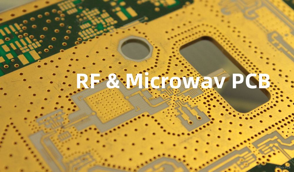
A ground plane is a large area of copper on a printed circuit board (PCB) that serves as a low-impedance return path for current in the circuit. It is typically located on one or more layers of the PCB and connected to the ground terminals of components. The ground plane helps to:
- Reduce electromagnetic interference (EMI) by providing a low-impedance return path for high-frequency currents
- Improve signal integrity by minimizing ground bounce and voltage differentials across the board
- Distribute heat evenly across the PCB, acting as a heat sink for power-dissipating components
- Simplify routing by providing a consistent reference point for signals
Types of Ground Planes
There are several types of ground planes used in PCB design, depending on the requirements of the circuit and the constraints of the board layout:
| Type | Description | Advantages | Disadvantages |
|---|---|---|---|
| Solid Plane | A continuous layer of copper covering most of the PCB area | – Lowest impedance – Best EMI suppression – Simplifies routing |
– May limit component placement – Requires careful planning of via locations |
| Gridded Plane | A mesh of copper traces forming a grid pattern | – Allows more flexibility in component placement – Can be used on multiple layers |
– Higher impedance than solid plane – May require additional vias for connections |
| Split Plane | Separate ground planes for analog and digital sections of the circuit | – Isolates sensitive analog circuits from digital noise – Allows optimization of each section |
– Requires careful design of the split – May complicate routing and increase board size |
Designing with Ground Planes
Component Placement and Routing
When designing a PCB with a ground plane, it’s important to consider the placement of components and the routing of traces to minimize the distance between the component ground pins and the ground plane. This helps to reduce inductance and improve signal integrity.
- Place decoupling capacitors close to the power pins of ICs to minimize the loop area between the capacitor and the ground plane
- Use wide, short traces for power and ground connections to minimize resistance and inductance
- Avoid routing signals over split planes or gaps in the ground plane, as this can cause discontinuities and reflections
Via Stitching and Grounding
Via stitching is the practice of placing multiple vias connecting the ground planes on different layers of the PCB. This helps to:
- Reduce ground bounce by providing low-impedance paths between layers
- Improve heat dissipation by allowing heat to flow through the vias to other layers
- Enhance mechanical stability by holding the layers together
When placing vias for grounding, consider the following guidelines:
- Place vias near the ground pins of components to minimize loop area
- Use a sufficient number of vias to handle the expected current flow without causing voltage drops
- Avoid placing vias too close to signal traces, as this can cause coupling and crosstalk
EMI Reduction Techniques
In addition to providing a low-impedance return path, ground planes can also help to reduce EMI by acting as a shield against radiated emissions. To maximize the shielding effectiveness of the ground plane:
- Use a solid plane rather than a gridded or split plane whenever possible
- Minimize gaps and slots in the ground plane, as these can act as antennas for EMI
- Use stitching capacitors to connect floating metal areas (such as connector shells) to the ground plane
- Consider using guard traces or co-planar waveguides for sensitive signals to minimize coupling to the ground plane
Ground Plane Simulation and Analysis
Before finalizing your PCB layout, it’s important to simulate and analyze the performance of the ground plane to ensure that it meets the requirements of your circuit. There are several tools and techniques available for ground plane analysis:
Electromagnetic Field Solvers
EM field solvers are software tools that use numerical methods (such as finite element analysis or method of moments) to calculate the electromagnetic fields and currents in a PCB structure. These tools can help to:
- Visualize current density and voltage distributions on the ground plane
- Identify areas of high impedance or resonance that may cause signal integrity issues
- Optimize via placement and grounding strategies for best performance
Some popular EM field solvers for PCB analysis include:
- Ansys HFSS
- Keysight EMPro
- CST Studio Suite
Power Integrity Analysis
Power integrity analysis focuses on the behavior of the power distribution network (PDN) in the PCB, including the ground plane. It helps to ensure that the PDN can deliver stable, clean power to all the components on the board. Power integrity analysis typically involves:
- Calculating the impedance of the PDN over frequency to identify resonances and anti-resonances
- Simulating the transient response of the PDN to switching loads to check for voltage ripple and ground bounce
- Optimizing decoupling capacitor placement and values to minimize impedance and supply noise
Some tools for power integrity analysis include:
- Cadence Sigrity PowerDC
- Mentor Graphics HyperLynx PI
- Altium Designer Power Integrity Extension
Signal Integrity Analysis
Signal integrity analysis looks at the quality of the signals transmitted through the PCB, including the effects of the ground plane on signal propagation. It helps to identify and mitigate issues such as:
- Reflections and ringing caused by impedance mismatches
- Crosstalk and coupling between signals and the ground plane
- Attenuation and distortion due to losses in the dielectric and conductor materials
Signal integrity analysis often involves:
- Time-domain reflectometry (TDR) to measure impedance and identify discontinuities
- Eye diagram analysis to visualize the quality of the received signal
- S-parameter measurements to characterize the frequency response of the channel
Some tools for signal integrity analysis include:
- Keysight ADS
- Ansys PathFinder
- Mentor Graphics HyperLynx SI

Best Practices for Ground Plane Design
To ensure the best performance and reliability of your PCB with a ground plane, follow these best practices:
- Use a solid ground plane whenever possible, and minimize gaps and slots
- Place decoupling capacitors close to the power pins of ICs, with short traces to the ground plane
- Use via stitching to connect ground planes on different layers and reduce ground bounce
- Avoid routing signals over split planes or gaps in the ground plane
- Use guard traces or co-planar waveguides for sensitive signals to minimize coupling
- Simulate and analyze the ground plane performance using EM field solvers, power integrity, and signal integrity tools
- Follow the manufacturer’s recommendations for layer stackup and material selection to optimize the ground plane performance
FAQ
1. What is the difference between a ground plane and a power plane?
A ground plane is a continuous layer of copper connected to the ground (0V) potential of the circuit, while a power plane is a similar layer connected to a positive supply voltage (such as +5V or +3.3V). Both planes serve as low-impedance reference points for signals and help to distribute current evenly across the board.
2. Can I use a ground plane on a single-layer PCB?
Yes, you can use a ground plane on a single-layer PCB, but it will be a bit different from a multi-layer board. On a single-layer PCB, the ground plane is typically a large area of copper on the same side as the components and traces, rather than a separate layer. It may not provide the same level of EMI suppression and signal integrity as a dedicated ground plane layer, but it can still help to improve the performance of the circuit.
3. How do I determine the thickness of the ground plane?
The thickness of the ground plane depends on several factors, including the expected current flow, the size of the PCB, and the manufacturing constraints. In general, a thicker ground plane will have lower impedance and better current-carrying capacity, but it may also increase the cost and weight of the board. A typical thickness for a ground plane in a multi-layer PCB is 0.5 oz to 2 oz of copper (17 μm to 70 μm).
4. What is the difference between a gridded ground plane and a solid ground plane?
A gridded ground plane is a mesh of copper traces forming a grid pattern, while a solid ground plane is a continuous layer of copper covering most of the PCB area. A gridded plane has higher impedance than a solid plane, but it allows more flexibility in component placement and routing. A solid plane provides the best EMI suppression and signal integrity, but it may limit the placement of components and vias.
5. How do I connect the ground pins of components to the ground plane?
To connect the ground pins of components to the ground plane, you should use short, wide traces and place the components as close to the ground plane as possible. This minimizes the inductance and impedance of the connection and helps to reduce ground bounce and EMI. You can also use via stitching to connect the ground pins directly to the ground plane on other layers of the board.

No responses yet