Introduction to Laser Direct Imaging (LDI) in PCB Manufacturing
Laser Direct Imaging (LDI) is a cutting-edge technology used in the fabrication of Printed Circuit Boards (PCBs). This innovative method has revolutionized the PCB manufacturing process by offering high precision, accuracy, and efficiency compared to traditional imaging techniques. RAYPCB, a leading PCB manufacturer, has embraced LDI technology to deliver superior quality PCBs to its customers.
In this comprehensive article, we will delve into the intricacies of Laser Direct Imaging, its advantages over conventional methods, and how RAYPCB leverages this technology to produce top-notch PCBs.
What is Laser Direct Imaging?
Laser Direct Imaging is a process that uses high-powered lasers to directly transfer the PCB design onto the photoresist-coated copper surface of the PCB Substrate. This process eliminates the need for traditional photomasks, which are used in conventional PCB imaging methods.
In LDI, the laser beam is precisely controlled and guided by a computer system that reads the PCB design data. The laser selectively exposes the photoresist layer, creating a highly accurate and detailed image of the desired circuit pattern.
Advantages of Laser Direct Imaging over Traditional Methods
Laser Direct Imaging offers several significant advantages over traditional PCB imaging methods, such as:
-
Higher Precision and Accuracy: LDI enables the creation of ultra-fine features and high-density interconnects (HDI) with exceptional precision and accuracy. The laser beam can achieve a resolution of up to 25 microns, ensuring that even the most intricate designs are reproduced faithfully.
-
Improved Efficiency: By eliminating the need for photomasks, LDI streamlines the PCB manufacturing process, reducing the number of steps involved. This leads to faster turnaround times and increased production efficiency.
-
Cost-Effectiveness: The elimination of photomasks also results in cost savings, as the expense associated with creating and maintaining these masks is removed from the equation. Additionally, LDI reduces material waste and minimizes the need for rework, further enhancing cost-effectiveness.
-
Flexibility in Design Changes: With LDI, design changes can be easily accommodated without the need to create new photomasks. This flexibility allows for quick iterations and adaptations, reducing lead times and enabling faster time-to-market for PCB designs.
-
Enhanced Quality Control: LDI incorporates advanced process control mechanisms, ensuring consistent and repeatable results. The automated nature of the process minimizes the risk of human error, resulting in higher quality PCBs with fewer defects.
The LDI Process at RAYPCB
RAYPCB has invested in state-of-the-art Laser Direct Imaging systems to offer its customers the benefits of this cutting-edge technology. Let’s take a closer look at the LDI process at RAYPCB:
1. Design Data Preparation
The first step in the LDI process is the preparation of the PCB design data. RAYPCB’s experienced engineering team reviews the customer’s design files and ensures that they are optimized for LDI. Any necessary adjustments or modifications are made in consultation with the customer to guarantee the best possible results.
2. Substrate Preparation
The PCB substrate, typically made of FR-4 or other high-quality materials, is carefully cleaned and prepared for the application of the photoresist layer. RAYPCB uses advanced cleaning techniques to ensure a contaminant-free surface, which is essential for optimal imaging results.
3. Photoresist Coating
A thin layer of photoresist is uniformly applied to the copper surface of the PCB substrate. RAYPCB employs precision coating equipment to ensure a consistent and even distribution of the photoresist, which is crucial for achieving high-quality imaging.
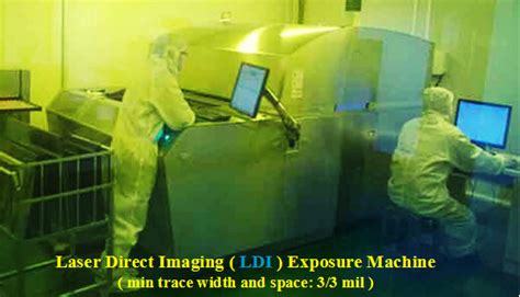
4. Laser Direct Imaging
The coated PCB substrate is then placed in the LDI machine, where the high-powered laser beam selectively exposes the photoresist layer according to the PCB design data. The laser is precisely controlled by a computer system that reads the design files and guides the beam to create a highly accurate image of the desired circuit pattern.
5. Development
After the laser exposure, the PCB substrate undergoes a development process. The exposed areas of the photoresist are removed, leaving behind a precise image of the circuit pattern on the copper surface. RAYPCB uses advanced development solutions and techniques to ensure sharp and well-defined features.
6. Etching
The developed PCB substrate is then subjected to an etching process, where the unwanted copper is removed, leaving behind the desired circuit traces. RAYPCB employs high-quality etching solutions and strict process controls to ensure accurate and consistent results.
7. Stripping and Cleaning
After etching, the remaining photoresist is stripped away, and the PCB substrate is thoroughly cleaned. RAYPCB uses eco-friendly stripping solutions and advanced cleaning methods to remove any residues and ensure a pristine surface for subsequent processing steps.

Benefits of LDI for RAYPCB’s Customers
By adopting Laser Direct Imaging technology, RAYPCB offers its customers a range of benefits, including:
-
Superior Quality PCBs: LDI enables RAYPCB to produce PCBs with exceptional precision, accuracy, and consistency. Customers can expect high-quality boards with fine features, HDI capabilities, and minimal defects.
-
Faster Turnaround Times: The streamlined LDI process allows RAYPCB to deliver PCBs to customers more quickly, reducing lead times and enabling faster time-to-market for their products.
-
Cost-Effective Solutions: By eliminating the need for photomasks and reducing material waste, LDI helps RAYPCB offer cost-effective PCB Solutions to its customers. This is particularly beneficial for low-volume and prototype productions.
-
Flexibility in Design Changes: RAYPCB’s LDI capabilities allow customers to make design changes easily and quickly, without incurring additional costs or delays associated with traditional imaging methods.
-
Environmentally Friendly: LDI is an environmentally friendly process that reduces waste and minimizes the use of harmful chemicals. By choosing RAYPCB’s LDI-manufactured PCBs, customers can contribute to a greener and more sustainable future.

Frequently Asked Questions (FAQ)
- What is the minimum feature size achievable with LDI at RAYPCB?
-
RAYPCB’s LDI systems can achieve a minimum feature size of 25 microns, enabling the creation of highly intricate and dense PCB designs.
-
Can LDI handle both rigid and flexible PCBs?
-
Yes, LDI technology can be used for both rigid and flexible PCB Fabrication. RAYPCB offers LDI services for a wide range of PCB Types and materials.
-
Is LDI suitable for high-volume production?
-
While LDI is particularly beneficial for low-volume and prototype productions, it can also be used for high-volume manufacturing. RAYPCB’s advanced LDI systems and optimized processes ensure efficient and cost-effective production, even for larger quantities.
-
How does LDI compare to other PCB imaging methods in terms of cost?
-
LDI eliminates the need for expensive photomasks, which can significantly reduce costs, especially for low-volume productions. However, the initial investment in LDI equipment can be higher compared to traditional imaging methods. RAYPCB strives to offer competitive pricing and cost-effective solutions for its customers.
-
What file formats are compatible with RAYPCB’s LDI systems?
- RAYPCB’s LDI systems are compatible with industry-standard file formats, such as Gerber, ODB++, and DXF. The company’s experienced engineering team can work with customers to ensure that their design files are optimized for LDI processing.

Conclusion
Laser Direct Imaging is a groundbreaking technology that has transformed the PCB manufacturing landscape. By offering unparalleled precision, accuracy, and efficiency, LDI has become the preferred choice for businesses seeking high-quality PCBs with quick turnaround times and cost-effective solutions.
RAYPCB, as a leading PCB manufacturer, has embraced LDI technology to deliver superior PCBs to its customers. With state-of-the-art LDI systems, experienced engineers, and a commitment to quality, RAYPCB is well-positioned to meet the evolving needs of the electronics industry.
By choosing RAYPCB’s LDI-manufactured PCBs, customers can benefit from exceptional quality, faster lead times, design flexibility, and environmentally friendly solutions. As technology continues to advance, RAYPCB remains at the forefront, leveraging the power of Laser Direct Imaging to drive innovation and success for its customers.
For more information about RAYPCB’s LDI capabilities and how they can benefit your PCB projects, please visit https://www.raypcb.com or contact our sales team at [email protected].
No responses yet