Understanding HDI PCB Stackups
What is an HDI PCB?
An HDI PCB is a printed circuit board that features higher wiring density per unit area compared to traditional PCBs. This is achieved through the use of smaller vias, finer trace widths, and tighter spacing between components. HDI PCBs enable the design of more compact and lightweight electronic devices while maintaining high performance and reliability.
HDI Stackup Nomenclature
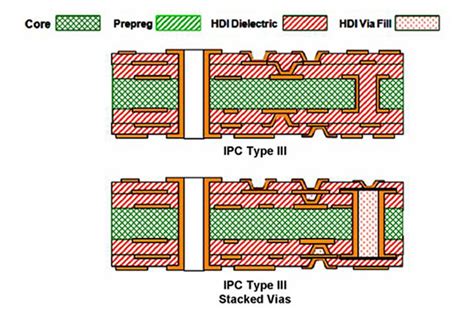
HDI Stackups are typically described using a nomenclature that indicates the number of copper layers and the presence of microvias. The format is as follows:
X+N+X
Where:
– X represents the number of copper layers with microvias
– N represents the number of copper layers without microvias
For example, a 1+N+1 stackup consists of two outer copper layers with microvias and N inner copper layers without microvias.
Common HDI Stackups
The following table summarizes the most common HDI stackups:
| Stackup | Description |
|---|---|
| 1+N+1 | Two Outer Layers with microvias, N inner layers |
| 2+N+2 | Four outer layers with microvias (two on each side), N inner layers |
| 3+N+3 | Six outer layers with microvias (three on each side), N inner layers |
| 4+N+4 | Eight outer layers with microvias (four on each side), N inner layers |
As the number of layers with microvias increases, the complexity of the PCB design and manufacturing process also increases.
Benefits of HDI PCBs
Miniaturization
One of the primary advantages of HDI PCBs is their ability to enable miniaturization. With smaller vias, finer traces, and tighter component spacing, HDI PCBs can accommodate more functionality in a smaller space. This is particularly important for applications such as smartphones, wearables, and IoT devices, where size and weight are critical factors.
Improved Signal Integrity
HDI PCBs offer improved signal integrity compared to traditional PCBs. The shorter signal paths and reduced layer count in HDI designs minimize signal reflections, crosstalk, and electromagnetic interference (EMI). This results in cleaner and more reliable signal transmission, which is essential for high-speed applications like 5G communication and high-performance computing.
Enhanced Thermal Management
The compact nature of HDI PCBs can pose challenges for thermal management. However, HDI stackups offer opportunities for efficient heat dissipation. By strategically placing thermal vias and using advanced materials with high thermal conductivity, HDI PCBs can effectively transfer heat away from critical components, ensuring optimal performance and reliability.
Cost Efficiency
Although HDI PCBs may have a higher initial cost compared to traditional PCBs, they offer long-term cost efficiency. The ability to integrate more functionality into a smaller form factor reduces the overall component count and assembly complexity. This leads to lower manufacturing and assembly costs, as well as reduced inventory management expenses.
HDI PCB Manufacturing Process
Design Considerations
Designing HDI PCBs requires careful consideration of various factors to ensure manufacturability and reliability. Some key design considerations include:
-
Via size and type: HDI PCBs typically use microvias, which have smaller diameters compared to traditional through-hole vias. The choice of via size and type (blind, buried, or through-hole) depends on the specific stackup and design requirements.
-
Trace width and spacing: HDI PCBs feature finer trace widths and tighter spacing between traces. Designers must adhere to the manufacturer’s design rules and guidelines to ensure proper signal integrity and manufacturability.
-
Component placement: The high density of HDI PCBs requires strategic component placement to optimize signal routing, thermal management, and assembly processes. Designers should consider factors such as component height, orientation, and spacing to avoid potential issues during manufacturing.
Material Selection
The choice of materials for HDI PCBs is crucial for achieving the desired performance and reliability. Some commonly used materials include:
-
Substrates: High-performance substrates like FR-4, Rogers, and Isola materials offer excellent electrical and mechanical properties suitable for HDI applications.
-
Copper foils: Thinner copper foils, such as 1/2 oz or 1/4 oz, are often used in HDI PCBs to enable finer trace widths and tighter spacing.
-
Solder masks: Liquid photoimageable (LPI) solder masks provide precise registration and resolution, making them ideal for HDI PCBs with fine features.
Fabrication Techniques
HDI PCB manufacturing involves several advanced fabrication techniques to achieve the required precision and reliability. Some key techniques include:
-
Laser drilling: Laser drilling is used to create microvias in HDI PCBs. The laser precisely removes the dielectric material to create small, high-quality vias.
-
Sequential lamination: HDI stackups often require sequential lamination, where layers are laminated in multiple steps to create the desired structure. This allows for the incorporation of microvias and fine features.
-
Plasma etching: Plasma etching is used to remove excess copper and create fine traces and spaces on the PCB surface. It offers high precision and consistency compared to traditional chemical etching.
Quality Control and Testing
Ensuring the quality and reliability of HDI PCBs requires rigorous quality control and testing procedures. Some essential steps include:
-
Automated optical inspection (AOI): AOI systems scan the PCB surface to detect any defects or anomalies, such as shorts, opens, or missing components.
-
Electrical testing: Various electrical tests, such as continuity, insulation resistance, and high-potential (hipot) tests, are performed to verify the electrical integrity of the PCB.
-
Microsectioning: Microsectioning involves cross-sectioning the PCB and examining the internal structure under a microscope to verify the integrity of vias, traces, and lamination.

One-Stop HDI PCB Manufacturing
Choosing a one-stop HDI PCB manufacturing partner offers several advantages over working with multiple vendors. Some key benefits include:
Streamlined Communication
With a one-stop solution, you have a single point of contact for all your HDI PCB needs. This streamlines communication and reduces the risk of misunderstandings or delays that can occur when coordinating with multiple vendors.
Consistent Quality
A one-stop manufacturer has full control over the entire manufacturing process, from design to fabrication to assembly. This ensures consistent quality throughout the process, as the manufacturer can optimize each step to meet your specific requirements.
Faster Turnaround Times
By handling all aspects of HDI PCB manufacturing in-house, a one-stop solution can offer faster turnaround times. There is no need to wait for components or sub-assemblies from multiple vendors, as everything is produced and integrated under one roof.
Cost Efficiency
Working with a one-stop manufacturer can be more cost-effective in the long run. You can benefit from economies of scale, as the manufacturer can optimize their processes and materials for your specific needs. Additionally, you can save on shipping and logistics costs by having a single source for your HDI PCBs.
Frequently Asked Questions (FAQ)
-
What is the minimum feature size achievable with HDI PCBs?
HDI PCBs can typically achieve minimum feature sizes of 50-75 microns for trace widths and spacing, and 100-150 microns for microvia diameters. However, the exact capabilities may vary depending on the manufacturer and the specific HDI stackup. -
Can HDI PCBs be used for high-power applications?
Yes, HDI PCBs can be designed for high-power applications by incorporating thicker copper layers, larger trace widths, and appropriate thermal management techniques. However, the specific power handling capability will depend on the design and the materials used. -
How do I choose the right HDI stackup for my application?
Choosing the right HDI stackup depends on factors such as the desired functionality, component density, signal integrity requirements, and cost constraints. It is recommended to consult with an experienced HDI PCB Manufacturer to discuss your specific needs and determine the most suitable stackup for your application. -
What are the challenges in designing HDI PCBs?
Designing HDI PCBs can be challenging due to the high density and fine features involved. Some common challenges include ensuring proper signal integrity, managing thermal dissipation, and adhering to the manufacturer’s design rules and guidelines. It is essential to work closely with the manufacturer and use advanced PCB design tools to overcome these challenges. -
How long does it typically take to manufacture HDI PCBs?
The manufacturing time for HDI PCBs can vary depending on the complexity of the design, the chosen stackup, and the manufacturer’s capabilities. Typically, lead times range from 2-4 weeks for prototypes and small batches, and 4-8 weeks for larger production runs. However, expedited services may be available for urgent projects.
Conclusion
HDI PCB manufacturing has revolutionized the electronics industry by enabling the creation of compact, high-performance devices. With stackups ranging from 1+N+1 to 4+N+4, HDI PCBs offer versatile solutions for a wide range of applications. Choosing a one-stop HDI PCB manufacturing partner can streamline the process, ensure consistent quality, and provide cost efficiency.
When embarking on an HDI PCB project, it is crucial to consider factors such as design requirements, material selection, and manufacturing capabilities. Working closely with an experienced HDI PCB manufacturer can help you navigate the complexities of HDI design and manufacturing, ensuring the success of your project.
As technology continues to advance, the demand for HDI PCBs is expected to grow. By understanding the intricacies of HDI PCB manufacturing and partnering with a reliable one-stop solution provider, you can stay ahead of the curve and bring your innovative ideas to life.

No responses yet