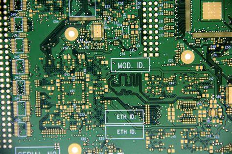
What is HDI PCB?
HDI (High Density Interconnect) PCB is a type of printed circuit board that features a higher wiring density per unit area compared to conventional PCBs. This is achieved through the use of finer traces, smaller vias, and advanced manufacturing techniques. HDI PCBs allow for the miniaturization of electronic devices while maintaining or improving their functionality and performance.
The main characteristics of HDI PCBs include:
– Fine pitch traces (less than 100 μm)
– Small vias (less than 150 μm)
– High layer count (typically 8 or more)
– Thin dielectric materials
– Blind and buried vias
– Sequential lamination process
Advantages of HDI PCBs
HDI PCBs offer several advantages over traditional PCBs:
-
Miniaturization: HDI technology enables the design of smaller and more compact electronic devices, which is crucial in industries such as consumer electronics, aerospace, and medical devices.
-
Improved signal integrity: The shorter signal paths and reduced parasitic capacitance in HDI PCBs lead to improved signal integrity, which is essential for high-speed applications.
-
Increased functionality: With a higher density of interconnects, HDI PCBs can accommodate more components and features in a smaller space, enabling the development of more sophisticated and multifunctional devices.
-
Reduced power consumption: The shorter signal paths in HDI PCBs result in lower power consumption, which is particularly important for battery-powered devices.
-
Enhanced reliability: HDI PCBs employ advanced manufacturing techniques and materials that contribute to improved reliability and durability of the final product.
Applications of HDI PCBs
HDI PCBs find applications in various industries and products, such as:
- Smartphones and tablets
- Wearable devices
- Medical implants and devices
- Aerospace and military electronics
- Automotive electronics
- IoT devices
- High-performance computing
HDI PCB Manufacturing Process
The manufacturing process of HDI PCBs involves several steps and advanced techniques to achieve the high density of interconnects. The main stages of HDI PCB manufacturing include:
-
Material selection: The choice of substrate material, copper foil, and dielectric materials is crucial for HDI PCBs. Common materials include FR-4, polyimide, and high-Tg laminates.
-
Patterning: The circuit pattern is transferred onto the copper-clad laminate using photolithography or laser direct imaging (LDI) techniques. The fine features of HDI PCBs require high-resolution imaging systems.
-
Etching: The unwanted copper is removed using chemical etching, leaving behind the desired circuit pattern.
-
Lamination: Multiple layers of patterned copper and dielectric materials are laminated together using heat and pressure to form a multi-layer PCB stack.
-
Drilling: Mechanical or laser drilling is used to create through-holes and vias in the PCB stack. HDI PCBs often employ blind and buried vias, which require precise depth control during drilling.
-
Plating: The drilled holes are plated with copper to establish electrical connections between layers. Additional plating steps, such as Via Filling or capping, may be required for HDI PCBs.
-
Surface finishing: A surface finish, such as ENIG (Electroless Nickel Immersion Gold) or ENEPIG (Electroless Nickel Electroless Palladium Immersion Gold), is applied to protect the exposed copper and facilitate component assembly.
-
Solder mask and silkscreen: A solder mask is applied to protect the circuitry, while silkscreen printing is used for component identification and labeling.
-
Electrical testing: The manufactured HDI PCBs undergo rigorous electrical testing to ensure functionality and compliance with design specifications.
HDI PCB Design Considerations
Designing HDI PCBs requires careful consideration of various factors to ensure optimal performance and manufacturability. Some key design considerations include:
-
Signal integrity: HDI PCBs must be designed with signal integrity in mind, taking into account factors such as impedance control, crosstalk, and electromagnetic interference (EMI).
-
Thermal management: The high density of components and interconnects in HDI PCBs can lead to increased heat generation. Proper thermal management, including the use of thermal vias and heat spreaders, is essential to ensure reliable operation.
-
Via structure: The choice of via structure (through, blind, or buried) and their placement is critical for HDI PCBs. Designers must consider the manufacturability and cost implications of different via configurations.
-
Layer stackup: The layer stackup of an HDI PCB must be carefully designed to optimize signal routing, impedance control, and power distribution. The use of thin dielectric materials and strategic placement of power and Ground Planes is crucial.
-
DFM (Design for Manufacturability): HDI PCB designers must adhere to DFM guidelines to ensure that the design can be efficiently and reliably manufactured. This includes considering minimum feature sizes, clearances, and tolerances specific to HDI fabrication processes.

HDI PCB Testing and Inspection
To ensure the quality and reliability of HDI PCBs, various testing and inspection methods are employed throughout the manufacturing process and after fabrication. Some common testing and inspection techniques include:
-
Automated Optical Inspection (AOI): AOI systems use high-resolution cameras and image processing algorithms to detect surface defects, such as missing components, solder bridges, or incorrect component placement.
-
X-ray Inspection: X-ray imaging is used to inspect the internal structure of HDI PCBs, particularly for hidden features such as blind and buried vias, and to detect voids or other defects in solder joints.
-
In-Circuit Testing (ICT): ICT involves the use of a bed-of-nails fixture to make electrical contact with specific points on the PCB and verify the proper functioning of individual components and circuits.
-
Flying Probe Testing: Flying probe testers use movable probes to make electrical contact with test points on the PCB surface, allowing for rapid testing of circuit continuity and component functionality without the need for a custom fixture.
-
Boundary Scan Testing: Also known as JTAG testing, boundary scan testing uses a built-in test architecture to verify the interconnections between digital components on the PCB.
-
Functional Testing: Functional testing involves powering up the assembLED PCB and verifying its operation under real-world conditions, often using automated test equipment (ATE) and custom test software.
By employing a combination of these testing and inspection methods, manufacturers can identify and address defects early in the production process, ensuring the delivery of high-quality HDI PCBs to their customers.

Future Trends in HDI PCB Technology
As electronic devices continue to evolve and demand for miniaturization and enhanced functionality grows, HDI PCB technology is expected to advance further. Some future trends in HDI PCB technology include:
-
Increased layer count: The number of layers in HDI PCBs is expected to increase, with some designs potentially featuring 16 or more layers to accommodate complex circuitry and higher interconnect densities.
-
Finer pitch and smaller vias: Advancements in manufacturing processes will enable even finer trace widths and smaller vias, allowing for greater miniaturization and higher component densities.
-
Advanced materials: The development of new substrate materials, such as low-loss dielectrics and high-performance laminates, will support the design of HDI PCBs for high-speed and high-frequency applications.
-
Embedded components: The integration of passive components, such as resistors and capacitors, directly into the PCB substrate will further increase component density and reduce the overall size of electronic devices.
-
3D packaging: The use of 3D packaging techniques, such as package-on-package (PoP) and through-silicon via (TSV) technology, will enable the vertical stacking of multiple HDI PCBs, leading to even greater miniaturization and functionality.
-
Intelligent PCBs: The incorporation of sensors, microcontrollers, and other smart components directly onto HDI PCBs will give rise to intelligent and self-monitoring electronic systems.
As HDI PCB technology continues to evolve, close collaboration between designers, manufacturers, and material suppliers will be essential to overcome challenges and drive innovation in the electronics industry.

Frequently Asked Questions (FAQ)
-
What is the difference between HDI PCBs and traditional PCBs?
HDI PCBs feature higher wiring density per unit area compared to traditional PCBs, achieved through the use of finer traces, smaller vias, and advanced manufacturing techniques. This allows for the miniaturization of electronic devices while maintaining or improving functionality and performance. -
What are the main advantages of using HDI PCBs?
The main advantages of HDI PCBs include miniaturization, improved signal integrity, increased functionality, reduced power consumption, and enhanced reliability. -
What industries commonly use HDI PCBs?
HDI PCBs are used in various industries, such as consumer electronics (smartphones and tablets), medical devices, aerospace and military electronics, automotive electronics, IoT devices, and high-performance computing. -
What are blind and buried vias, and why are they used in HDI PCBs?
Blind vias connect an outer layer to an inner layer without going through the entire PCB, while buried vias connect two or more inner layers without reaching the outer layers. These via types are used in HDI PCBs to increase interconnect density and minimize the PCB size. -
What are some key design considerations for HDI PCBs?
Key design considerations for HDI PCBs include signal integrity, thermal management, via structure, layer stackup, and design for manufacturability (DFM). Designers must carefully balance these factors to ensure optimal performance and reliable manufacturing of HDI PCBs.
In conclusion, HDI PCB technology represents a significant advancement in the world of printed circuit boards, enabling the development of smaller, more functional, and more reliable electronic devices. As the demand for miniaturization and enhanced performance continues to grow, HDI PCBs will play an increasingly crucial role in shaping the future of the electronics industry. By understanding the characteristics, manufacturing processes, design considerations, and testing methods associated with HDI PCBs, engineers and manufacturers can leverage this technology to create innovative and high-quality electronic products that meet the evolving needs of consumers and businesses alike.
No responses yet