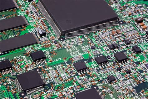
Introduction to PCBA Manufacturing
Printed Circuit Board Assembly (PCBA) manufacturing is a complex process that involves the assembly of electronic components onto a printed circuit board (PCB). The PCBA manufacturing process is crucial in the production of electronic devices, as it determines the functionality, reliability, and quality of the final product. In this article, we will take an in-depth look at the various stages involved in the PCBA manufacturing process.
Overview of the PCBA Manufacturing Process
The PCBA manufacturing process can be divided into several key stages, each of which plays a critical role in the production of high-quality electronic assemblies. These stages include:
- PCB Design and Fabrication
- Component Sourcing and Procurement
- Solder Paste Printing
- Component Placement
- Reflow Soldering
- Inspection and Testing
- Conformal Coating and Potting
- Final Assembly and Packaging
Let’s explore each of these stages in more detail.
PCB Design and Fabrication
The first stage of the PCBA manufacturing process is PCB design and fabrication. This stage involves the creation of a detailed layout of the electronic circuit, which is then used to manufacture the bare PCB. The PCB design process typically involves the following steps:
- Schematic Design: The electronic circuit is designed using specialized software, such as Altium Designer or OrCAD.
- Component Selection: The appropriate electronic components are selected based on the circuit requirements and design specifications.
- PCB Layout: The component placement and routing of the traces are determined to ensure optimal performance and manufacturability.
- Design Verification: The PCB design is checked for errors and potential issues, such as signal integrity problems or manufacturing constraints.
- Gerber File Generation: The final PCB design is converted into Gerber Files, which are used by PCB fabrication houses to manufacture the bare PCBs.
Once the PCB design is finalized, the bare PCBs are fabricated using a variety of processes, including:
- Etching: The unwanted copper is removed from the PCB substrate to create the desired circuit pattern.
- Drilling: Holes are drilled into the PCB to accommodate through-hole components and vias.
- Plating: The holes are plated with a conductive material, typically copper, to ensure electrical connectivity.
- Solder Mask Application: A protective layer, known as solder mask, is applied to the PCB surface to prevent short circuits and improve the assembly process.
- Silkscreen Printing: Text and symbols are printed onto the PCB surface to aid in component placement and identification.
Component Sourcing and Procurement
The next stage in the PCBA manufacturing process is component sourcing and procurement. This stage involves identifying and purchasing the electronic components required for the assembly. Key aspects of component sourcing and procurement include:
- Bill of Materials (BOM) Creation: A comprehensive list of all the required components, along with their quantities and specifications, is created.
- Supplier Selection: Reliable suppliers are identified and selected based on factors such as cost, quality, lead time, and minimum order quantities.
- Component Availability: The availability of the required components is checked to ensure that they can be procured in the necessary quantities and timeframes.
- Quality Control: Incoming components are inspected to ensure that they meet the required specifications and are free from defects.
Effective component sourcing and procurement are essential for ensuring the timely and cost-effective production of high-quality PCBAs.
Solder Paste Printing
Once the bare PCBs and components have been procured, the next stage in the PCBA manufacturing process is solder paste printing. This stage involves the application of solder paste, a mixture of tiny solder particles and flux, onto the PCB pads. The most common method for solder paste printing is stencil printing, which uses a metal stencil with apertures that correspond to the PCB pads. The stencil is aligned with the PCB, and solder paste is applied using a squeegee or automated printer.
Key factors that affect the quality of solder paste printing include:
- Stencil Design: The stencil aperture size, shape, and thickness must be carefully designed to ensure the correct amount of solder paste is deposited on each pad.
- Solder Paste Properties: The solder paste must have the appropriate viscosity, particle size, and flux activity to ensure good printability and wetting.
- Printer Setup: The printer parameters, such as squeegee pressure, speed, and separation distance, must be optimized to achieve consistent and accurate solder paste deposits.
- Environmental Control: Temperature and humidity control are essential to maintain the stability and performance of the solder paste.
Proper solder paste printing is critical for ensuring reliable solder joints and preventing defects such as bridging, insufficient solder, or solder balls.
Component Placement
After solder paste printing, the next stage in the PCBA manufacturing process is component placement. This stage involves the precise placement of electronic components onto the PCB pads. Component placement can be performed manually, using tweezers and a magnifying lens, or automatically, using Pick-and-Place machines.
Automated component placement offers several advantages over manual placement, including:
- Speed: Pick-and-place machines can place components at rates of tens of thousands per hour, significantly reducing assembly time.
- Accuracy: Automated placement ensures consistent and precise component positioning, reducing the risk of placement errors.
- Flexibility: Pick-and-place machines can handle a wide range of component sizes and types, from small chip components to large connectors and modules.
Key factors that affect the quality of component placement include:
- Machine Calibration: Pick-and-place machines must be regularly calibrated to ensure accurate component positioning and alignment.
- Component Feeding: Components must be correctly oriented and fed into the pick-and-place machine to ensure reliable pickup and placement.
- Placement Programming: The placement program must be carefully developed and optimized to ensure efficient and accurate component placement.
- Fiducial Recognition: Fiducial markers on the PCB are used by the pick-and-place machine to align the board and ensure accurate component placement.
Accurate component placement is essential for ensuring proper electrical connections and preventing issues such as component misalignment or tombstoning.
Reflow Soldering
Once the components have been placed on the PCB, the next stage in the PCBA manufacturing process is reflow soldering. This stage involves the application of heat to melt the solder paste and form permanent electrical and mechanical connections between the components and the PCB pads. Reflow soldering is typically performed using a reflow oven, which exposes the PCBA to a controlled temperature profile.
The reflow soldering process can be divided into four main phases:
- Preheat: The PCBA is gradually heated to activate the flux and remove any moisture from the components and PCB.
- Thermal Soak: The temperature is maintained at a stable level to ensure that all components reach the same temperature and to allow the flux to clean the component leads and PCB pads.
- Reflow: The temperature is rapidly increased to melt the solder particles and form solder joints between the components and PCB pads.
- Cooling: The PCBA is cooled to solidify the solder joints and prevent thermal shock to the components.
Key factors that affect the quality of reflow soldering include:
- Temperature Profile: The reflow temperature profile must be carefully designed and controlled to ensure proper solder melting and joint formation without damaging the components or PCB.
- Atmosphere Control: Reflow ovens typically use nitrogen or other inert gases to prevent oxidation and improve solder joint quality.
- PCB Support: The PCB must be adequately supported during reflow to prevent warping or sagging, which can lead to component misalignment or poor solder joints.
- Thermal Management: Proper thermal management, including the use of thermal reliefs and heat sinks, is essential to prevent component damage during reflow.
Proper reflow soldering is critical for ensuring reliable and robust solder joints that can withstand the stresses of assembly, handling, and operation.
Inspection and Testing
After reflow soldering, the next stage in the PCBA manufacturing process is inspection and testing. This stage involves the verification of the assembled PCBA to ensure that it meets the required quality standards and functional specifications. Inspection and testing can be performed using a variety of methods, including:
- Visual Inspection: The PCBA is visually inspected for defects such as poor solder joints, bridging, component misalignment, or damage.
- Automated Optical Inspection (AOI): An automated system captures high-resolution images of the PCBA and compares them to a reference image to detect defects.
- X-Ray Inspection: X-ray imaging is used to inspect solder joints and components that are hidden from view, such as ball grid array (BGA) packages or through-hole components.
- In-Circuit Testing (ICT): The PCBA is placed in a fixture that makes electrical contact with the board, allowing the testing of individual components and circuits.
- Functional Testing: The PCBA is tested under real-world operating conditions to verify that it performs as intended and meets the required specifications.
Key factors that affect the effectiveness of inspection and testing include:
- Inspection Coverage: The inspection and testing methods must provide adequate coverage of the PCBA to detect potential defects or issues.
- Defect Classification: Defects must be accurately classified and prioritized based on their severity and potential impact on PCBA functionality and reliability.
- Test Coverage: Functional testing must be designed to cover all critical aspects of PCBA operation and performance.
- Traceability: Inspection and test results must be properly documented and traceable to individual PCBAs and production lots.
Thorough inspection and testing are essential for identifying and correcting defects early in the manufacturing process, reducing rework costs and improving overall PCBA quality and reliability.
Conformal Coating and Potting
In some cases, the PCBA manufacturing process may include additional steps such as conformal coating or potting to enhance the protection and reliability of the assembly. Conformal coating involves the application of a thin, protective layer of material, such as acrylic, silicone, or polyurethane, over the surface of the PCBA. This layer helps to protect the assembly from moisture, dust, chemicals, and other environmental factors that can degrade performance or cause failures.
Potting, on the other hand, involves the complete encapsulation of the PCBA in a solid compound, such as epoxy or silicone. Potting provides even greater protection than conformal coating, as it fully surrounds and supports the components and connections. Potting is often used in applications that require high levels of mechanical strength, thermal management, or resistance to harsh environments.
Key factors that affect the quality of conformal coating and potting include:
- Material Selection: The coating or potting material must be carefully selected based on the specific requirements of the application, such as temperature range, chemical resistance, or dielectric strength.
- Application Method: The coating or potting material must be applied using a suitable method, such as spraying, dipping, or dispensing, to ensure uniform coverage and thickness.
- Curing: The coating or potting material must be properly cured to achieve its desired properties and ensure good adhesion to the PCBA surface.
- Masking: Critical areas of the PCBA, such as connectors or test points, must be properly masked to prevent coating or potting material from interfering with their function.
Conformal coating and potting can significantly improve the reliability and durability of PCBAs, particularly in challenging operating environments.
Final Assembly and Packaging
The final stage in the PCBA manufacturing process is final assembly and packaging. This stage involves the integration of the PCBA into the final product or system, along with any additional components, hardware, or firmware. Final assembly and packaging may include steps such as:
- Mechanical Assembly: The PCBA is installed into the product enclosure or chassis, along with any required mounting hardware, connectors, or cables.
- Firmware Programming: Any required firmware or software is loaded onto the PCBA, and the assembly is configured and tested to ensure proper operation.
- Labeling and Marking: The PCBA or final product is labeled with relevant information such as part numbers, serial numbers, or certification marks.
- Packaging: The final product is packaged in appropriate materials, such as anti-static bags, foam, or boxes, to protect it during storage and shipping.
Key factors that affect the quality of final assembly and packaging include:
- Assembly Instructions: Clear and detailed assembly instructions must be provided to ensure consistent and accurate final assembly.
- Electrostatic Discharge (ESD) Protection: Proper ESD protection measures, such as grounding straps and anti-static materials, must be used to prevent damage to sensitive components during handling and assembly.
- Quality Control: Final inspection and testing must be performed to verify that the assembled product meets all functional and quality requirements.
- Packaging Design: Packaging materials and designs must be selected to provide adequate protection against shock, vibration, and environmental factors during storage and transportation.
Careful attention to final assembly and packaging helps to ensure that the PCBA and final product are delivered to the customer in optimal condition and ready for use.

Conclusion
The PCBA manufacturing process is a complex and multi-faceted endeavor that requires careful planning, execution, and quality control at every stage. From PCB design and fabrication to final assembly and packaging, each step plays a critical role in determining the functionality, reliability, and overall quality of the finished product.
By understanding the key stages and factors involved in PCBA manufacturing, engineers, managers, and technicians can work together to optimize the process, minimize defects and failures, and deliver high-quality electronic assemblies that meet the evolving needs of today’s markets and applications.

Frequently Asked Questions (FAQ)
- What is the difference between PCB and PCBA?
-
A PCB, or printed circuit board, is the bare board with conductive traces and pads, but without any components installed. A PCBA, or printed circuit board assembly, is a PCB that has been populated with electronic components and has undergone the solder reflow process to create electrical connections.
-
What are the most common defects encountered in PCBA manufacturing?
-
Some of the most common defects in PCBA manufacturing include poor solder joints (e.g., bridging, insufficient solder, or cold joints), component misalignment or shifting, damaged or missing components, and shorts or opens in the circuit traces. Other issues may include PCB warping, delamination, or contamination.
-
How can PCBA manufacturing defects be prevented or minimized?
-
PCBA manufacturing defects can be prevented or minimized through a combination of careful process control, regular equipment maintenance and calibration, thorough operator training, and robust quality inspection and testing procedures. The use of automated assembly equipment, such as pick-and-place machines and reflow ovens, can also help to improve consistency and reduce the risk of human error.
-
What are the benefits of using automated inspection methods, such as AOI or X-ray, in PCBA manufacturing?
-
Automated inspection methods, such as automated optical inspection (AOI) or X-ray inspection, offer several benefits in PCBA manufacturing. These include faster and more consistent defect detection, improved coverage and accuracy compared to manual inspection, and the ability to identify defects that may be hidden from view, such as those in BGA packages or under components. Automated inspection can also help to reduce labor costs and improve overall quality control.
-
How does the choice of solder paste and reflow profile affect the quality of solder joints in PCBA manufacturing?
- The choice of solder paste and reflow profile can have a significant impact on the quality of solder joints in PCBA manufacturing. Solder paste must be selected based on factors such as alloy composition, particle size, and flux activity to ensure good printability, wetting, and joint formation. The reflow profile, including the temperature ramp rates, soak times, and peak temperatures, must be carefully designed and controlled to ensure proper solder melting and joint formation without causing component or PCB damage. Improper solder paste or reflow profile selection can lead to defects such as poor wetting, bridging, or cold joints.

PCBA Manufacturing Process Overview
| Stage | Description | Key Factors |
|---|---|---|
| PCB Design and Fabrication | Creation of PCB layout and manufacturing of bare PCBs | – Schematic design – Component selection – PCB layout – Design verification – Gerber file generation |
| Component Sourcing and Procurement | Identification and purchase of required electronic components | – Bill of Materials (BOM) creation – Supplier selection – Component availability – Quality control |
| Solder Paste Printing | Application of solder paste onto PCB pads using stencil printing | – Stencil design – Solder paste properties – Printer setup – Environmental control |
| Component Placement | Precise placement of components onto PCB pads, either manually or using pick-and-place machines | – Machine calibration – Component feeding – Placement programming – Fiducial recognition |
| Reflow Soldering | Application of heat to melt solder paste and form solder joints | – Temperature profile – Atmosphere control – PCB support – Thermal management |
| Inspection and Testing | Verification of assembled PCBA quality and functionality | – Visual inspection – Automated optical inspection (AOI) – X-ray inspection – In-circuit testing (ICT) – Functional testing |
| Conformal Coating and Potting | Application of protective coatings or encapsulation to enhance PCBA |
No responses yet